Today, wireless data transmission permeates virtually every industry. This demand is driven primarily by commercial and residential computer networking, along with the extensive use of mobile devices and portables. Applications, like the Internet of Things (IoT) and Industrial IoT (IIoT), are also pushing the envelope for greater functionality and advanced capabilities.
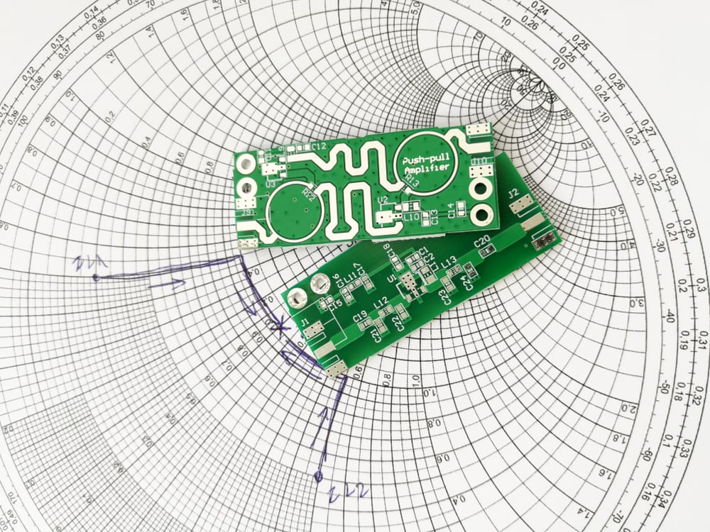
The common denominator for these uses is the reliance on electronic circuit boards for RF and microwave transmission and/or reception (TX/RX). And the antenna is a critical component for effective PCBA data and signal transmission. Tools; such as the Smith Chart, are helpful in choosing the best components for impedance matching. However, for optimization of complex TX/RX systems, more advanced tools are essential to select and implement the best antenna matching network design for your application and effectively manage product design cost.
Antenna Matching Network Design Techniques
The number of different circuits–or specific sets of components–that can be used for antenna matching is virtually endless. However, antenna matching network designs can be generally classified based on the number of elements used, as shown in the table below.
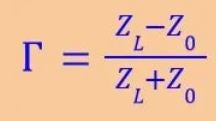
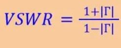
The goal of an antenna matching network is to match the antenna or load impedance with the signal generation or source impedance; such that maximum power is transferred to the antenna for radiation. Maximum power transfer occurs when energy losses and reflections between the source and load are eliminated or reduced.
Designing Antenna Impedance Matching Networks
Antenna matching network design ranges from simple to complex, depending on the desired operating parameters, defined below, for your application.
*Lossless transmission lines do not exist. However, they are a useful ideal perspective from which practical systems can be evaluated.
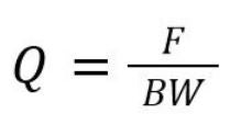
Practically, maximum power transfer requires that the source and load resistances are the same and reactances cancel each other (are equal and opposite). This condition occurs at a specific frequency. Therefore, another important design parameter is the quality or Q factor of the antenna matching network. This value is defined as shown below.
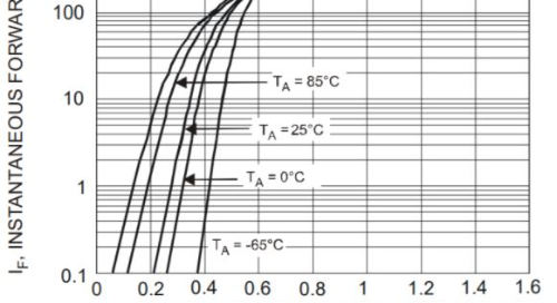
For some systems, choosing the appropriate component values of capacitance and inductance is fairly straightforward. And tools like the Smith Chart can aid you in readily selecting the best circuit elements. However, for complex systems determining the component values for lumped reactances can be quite challenging. Especially, since physical constraints often restrict the Q factor value.
For more information on designing antenna matching networks, see our how-to.
Achieving the Best Antenna Matching Design
As the applications for wireless transmission continue to expand, the performance requirements and physical constraints on the circuit boards that drive them continue to become more demanding. Consequently, designing antenna matching networks can easily escalate from the selection of a hand full of components to selecting the best values for a large number of complex network elements. Doing so can be time-consuming and significantly drive up PCBA develop costs.
In these cases, the best solution is to employ a product development tool that includes advanced capabilities to help optimize your antenna matching network design. AWR, which is developed specifically for designing and analyzing RF and microwave systems, is such an EDA support tool. With AWR, design and simulation of your antenna network is integrated to aid you in efficiently optimizing gain, frequency range, loss and other important parameters.
EMA Design Automation is a leading provider of the resources that engineers rely on to accelerate innovation. We provide solutions that include PCB design and analysis packages, custom integration software, and engineering expertise, which enable you to create more efficiently. For more information on antenna matching network design optimization and how we can help you or your team innovate faster, contact us.