Arguably, AI is the most influential concept to impact PCB development in recent years. The thrust to build smarter electronic products is observable everywhere. Further, the incorporation of intelligence into the design, manufacturing, and testing of circuit boards, which drive smart devices and systems, is continually increasing.
For PCB design, emphasis is placed on improving schematic capture and PCB layout tasks to achieve better development process quality, efficiency, and cost. To address these goals, circuit board design programs have become more robust. However, additional product development tools and techniques are often needed to supplement design program limitations. Making the best use of these enhancements requires optimization of these software integrations with your EDA tool.
Product Development Tools and Techniques for Enhanced PCB Design
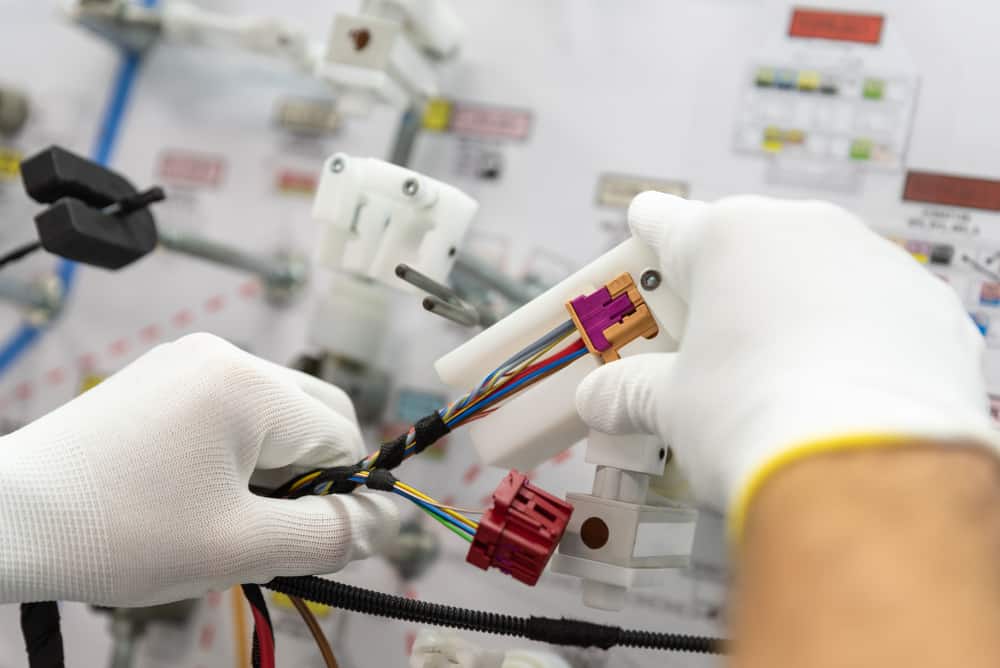
Gone are the days of the black box PCB development model, where board designers and manufacturers worked in isolation and had little knowledge of the other’s processes or intent. Today, it is acknowledged that CMs must understand design intent, and engineers must incorporate design for manufacturing and assembly practices for an efficient and quality board-building process. Manufacturability, however, does not guarantee operational and performance success.
The goals of PCB development optimization are to:
Ensure that your boards are built well and structurally reliable.
Satisfy the design performance objectives.
Minimize time and maximize ROI.
Your success in achieving these goals is greatly improved with the following functionalities and capabilities included in or integrated with your EDA tool.
⏫✅ – improve quality ⏬🕙 – reduce development time ⏬💲– lower development costs
Although not exhaustive, the list of electronic product development tools above does accurately illustrate the advanced support tools available to facilitate the optimization of your board design, manufacturing, and operation once deployed.
Optimizing Your EDA Software Integrations
Employing advanced product development tools and techniques into your PCB design will allow you to raise the quality of your process, achieve faster turnaround times, and lower costs. To realize these advantages, follow the guidelines below for the best integration with your board design program.
Optimizing your PCBA development process has to be a goal in today’s competitive electronics products industry. Fortunately, advanced product development tools and techniques exist to help you reach this goal.
EMA Design Automation is a leading provider of the resources that engineers rely on to accelerate innovation. We provide solutions that include PCB design and analysis packages, custom integration software, and engineering expertise, which enable you to create more efficiently. For more information on the benefits of product development tools and techniques and how we can help you or your team innovate faster, contact us.