Power is essential to circuit functionality and influences decisions throughout the PCB design process. Reducing power consumption can have a beneficial effect on the design, decreasing component costs and improving product efficiency; however, reducing power too much can lead to intermittent failures and poor circuit performance. It is important to verify the minimum power requirements that will produce proper circuit functionality to improve device success. With OrCAD PSpice Designer, you can:
- Improve reliability
- Improve efficiency
- Reduce power consumption
- Reduce energy requirements
- Extend battery life for mobile devices
- Reduce unwanted heat
- Lower cost
- Analyze the required power for optimal functionality
This quick how-to will provide step-by-step instructions on how to optimize power in PSpice and modify an amplifier design to work with a reduction in supply voltage.
To follow along, download the provided design above the table of contents.
How-To Video
Running a Simulation
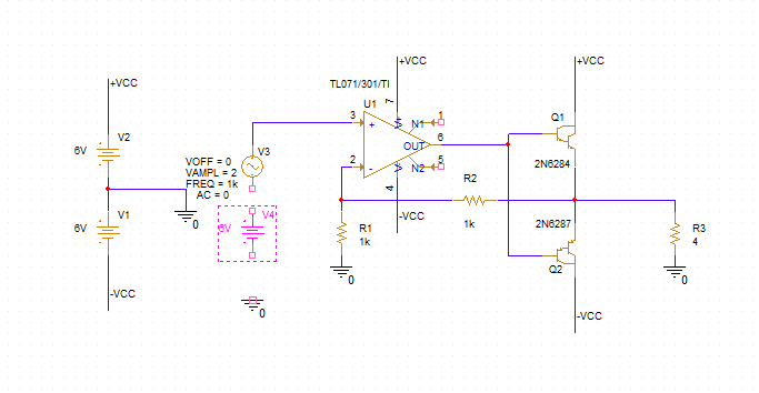
Step 1: Open the provided design in OrCAD PSpice Designer.
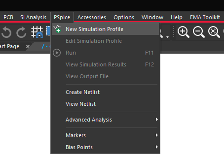
Step 2: Select PSpice > New Simulation Profile from the menu.
Step 3: Enter POWER_AMP as the new simulation name and click Create. The Simulation Settings window opens.
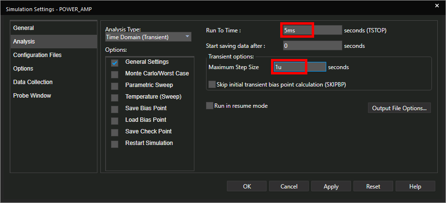
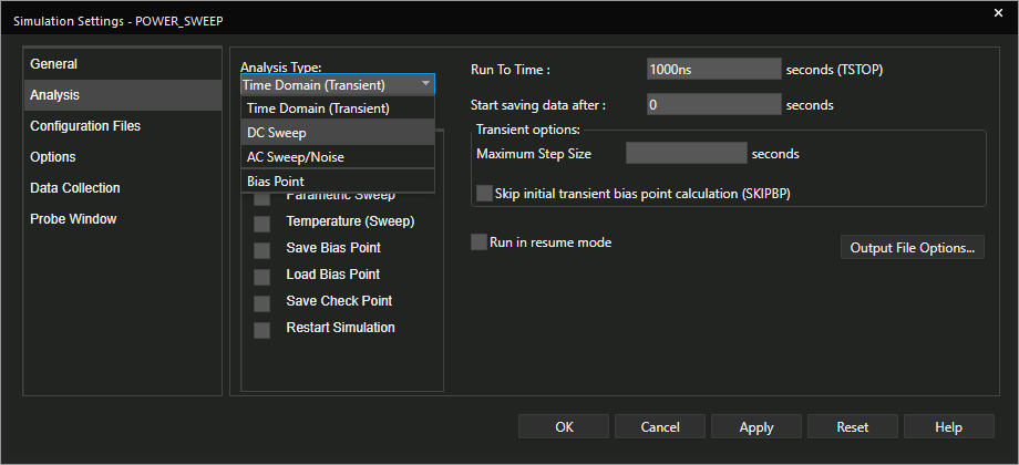
Step 4: Set the Run To Time to 5ms.
Step 5: Set the Maximum Step Size to 1u.
Note: This will set the maximum step size to 1 microsecond, producing a more accurate simulation.
Step 6: Click OK to create the simulation profile.
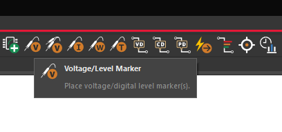
Step 7: Select the Voltage/Level Marker icon from the toolbar to place a probe.
Step 8: Click to place the probe on the output net. Right-click and select End Mode when finished.
Step 9: Select PSpice > Run from the menu to start the simulation.
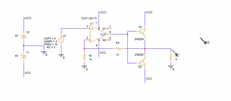
Step 10: View the simulation results. An amplified sine wave is shown, as expected.
Reducing Source Voltage
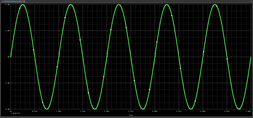
Step 11: Double-click the 9V value of V1 to change it.
Step 12: Enter a value of 6V and click OK.
Step 13: Double-click the value of V2. Enter 6V and click OK.
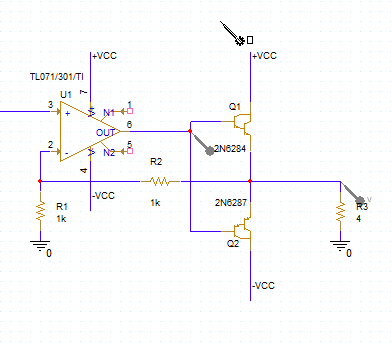
Step 14: Select the Voltage/Level Marker icon from the toolbar to place a probe. Place the probe at the bases of Q1 and Q2. Right-click and select End Mode.
Step 15: Select PSpice > Run from the menu.
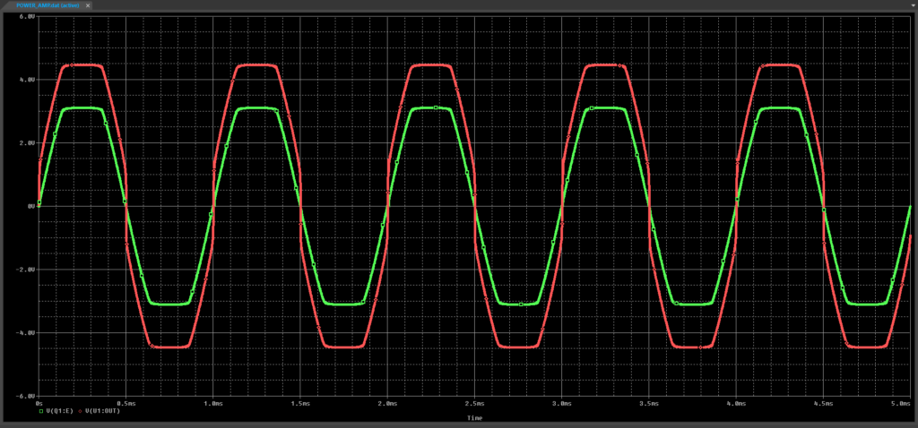
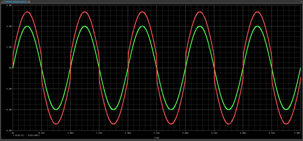
Step 16: View the simulation results.
Note: The output sine wave is green, and the base wave is red. The base voltage is clipped when the op-amp output reaches its upper limit, which clips the amplifier output as well. Note that this limit is under 4.5V, well under the limits of +6V and -6V.
Optimizing Performance
Step 17: Select PSpice > New Simulation Profile from the menu.
Step 18: Name the simulation profile POWER_SWEEP and click Create.
Step 19: In the Simulation Settings window, select DC Sweep from the Analysis Type dropdown.
Step 20: Under Sweep Variable, select Voltage Source and enter V2.
Step 21: Set the Sweep Type to Linear.
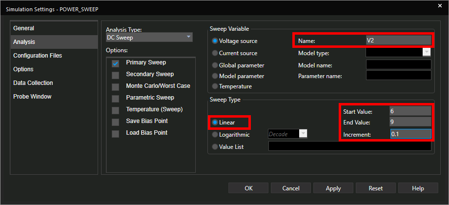
Step 22: Enter 6 for the Start Value, 9 for the End Value, and 0.1 for the Increment. Click OK.
Note: The AC source V3 will be analyzed as a short to ground with the DC sweep analysis. A DC component needs to be added.
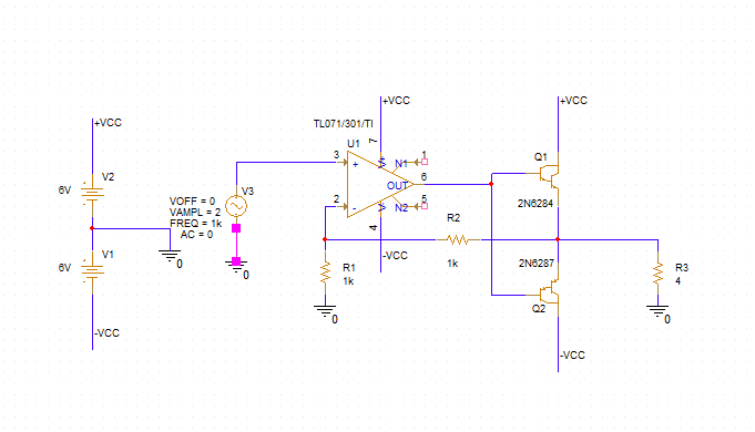
Step 23: Select the wire connecting V3 to ground. Press Delete on the keyboard to remove the connection.
Step 24: Click and drag the ground to move it down further as needed.
Step 25: Select V1 and press CTRL-C on the keyboard.
Step 26: Press CTRL-V and click to place the source between V3 and ground.
Step 27: Double-click the value of the newly placed source to change it.
Step 28: Set the value to 2V and click OK.
Note: This is the peak of the original input signal.
Step 29: Select Place > Wire from the menu, the Wire button from the toolbar, or press W on the keyboard.
Step 30: Click to connect the positive of source V4 to the lower terminal of V3. Press Escape on the keyboard when finished.
Step 31: Select the Voltage/Level Marker icon from the toolbar. Click to place the probe on the output net. Right-click and select End Mode when finished.
Step 32: Select PSpice > Run from the menu.
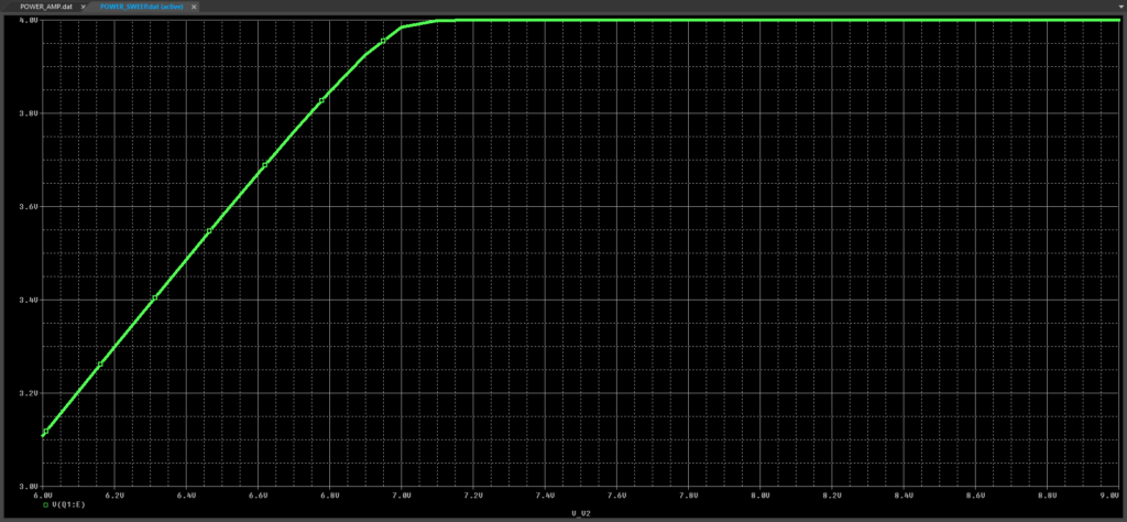
Step 33: View the simulation results. The output holds at a steady 4V when the input voltage is approximately 7.2V or greater.
Correcting the Supply Voltages
Step 34: Back in the schematic, select source V4 and press Delete on the keyboard.
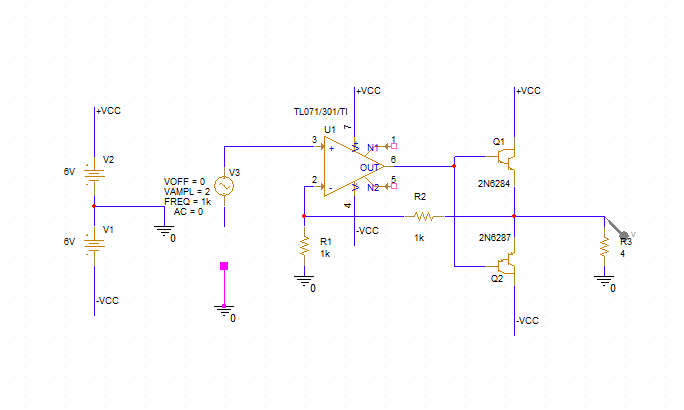
Step 35: Select the endpoint of the wire connected to ground. Click and drag to reconnect V3 to ground.
Step 36: Double-click the value of V1. Enter 7.2V and click OK.
Step 37: Double-click the value of V2. Enter 7.2V and click OK.
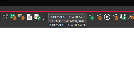
Step 38: Select SCHEMATIC1-POWER_AMP from the simulation selector dropdown.
Step 39: Select PSpice > Run from the menu.
Step 40: View the simulation results. The clipping has been resolved and the circuit is performing as intended.
Wrap Up & Next Steps
Improve reliability and efficiency of your PCB without overdesigning by analyzing the effects of power on circuit performance with OrCAD PSpice Designer. Test out this feature and more with a free trial of OrCAD.
