With the ever-increasing complexity of today’s designs and shrinking mechanical housing requirements, it is important to guarantee all the components will fit on the PCB. Finding out the components selected won’t adhere to the mechanical requirements or allow enough room for routing during the PCB layout may push the project off track and delay the product release. Easily estimate the board space required by calculating the area of the board which will be occupied by components and determine if any components need to be changed during the schematic design with the CircuitFit app.
This how-to will provide step-by-step instructions on how to use the CircuitFit app in OrCAD Capture. In order for CircuitFit to be used the following requirements must be met:
- OrCAD PCB Designer installed
- Java Version 8 installed
- PCB Footprints assigned
- Netlist created
How-to Video
Opening CircuitFit
Step 1: Open the desired design in OrCAD Capture.
Note: The design must have PCB footprints assigned.
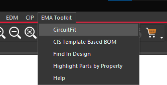
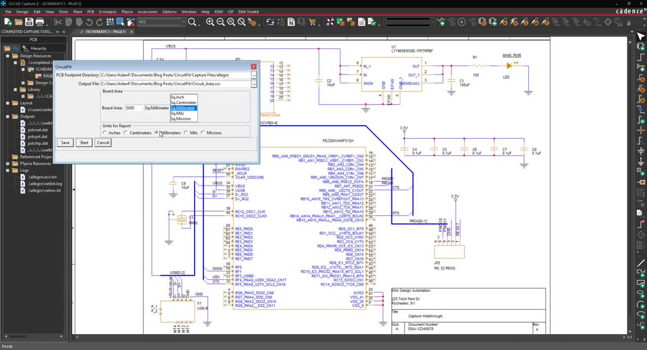
Step 2: Select EMA Toolkit > CircuitFit from the menu. The CircuitFit window will open.
Configuring CircuitFit
Step 3: Enter the board area into the field labeled Board Area.
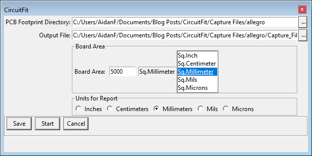
Step 4: Select the unit of the board area from the list to the right of the Board Area field.
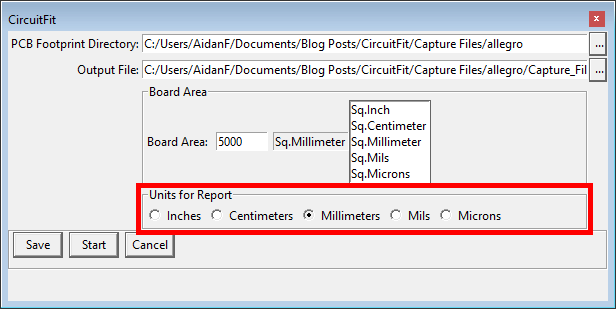
Step 5: Select the desired units for the measurements in the report.
Running the CircuitFit App
Step 6: Click Start to run the analysis.
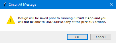
Step 7: A prompt will appear, with the message that the design will be saved prior to running CircuitFit. Click OK.
Determining Space Used by Components
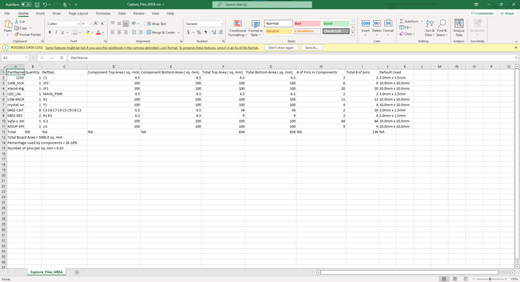
Step 8: When the analysis finishes, the resulting CSV file will open in Microsoft Excel with the total area of the board used by components.
Note: The following information is included in the CSV file for each part found:
- PartName: The PCB Footprint name
- Quantity: The number or occurrences that the footprint was used in the design.
- RefDes: The Reference Designators for all parts found with the specified footprint.
- Component Top Area (Units): The area that the component will take up on the top side of the board.
- Component Bottom Area (Units): The area that the component will take up on the bottom side of the board. (e.g. Through hole parts will have area in the top and bottom.)
- Total Top Area (Units): The product of quantity and the component top area.
- Total Bottom Area (Units): The product of quantity and the component bottom area.
- # of Pins in Components: The number of pins that a component has.
- Total # of pins: The product of quantity and the number of pins in the component.
- Default Used: The default size used in the calculations if a default has been used.
A summary of the calculations is also provided at the bottom of the .CSV file:
- The total board area: The board area used in the calculations.
- The percentage used for the board: The ratio of the sum of top and bottom component areas to the board area.
- Number of pins per sq. unit: The pin density which is the ratio of the total pin count to the board area.
Wrap Up & Next Steps
Easily determine how much space the components will occupy on the PCB during the schematic design when component change is easiest using the CircuitFit App in OrCAD Capture. This app and others are part of the EMA Toolkit, one of the benefits of EMA Support +. The EMA Support + program is available to all EMA customers on active support and includes additional benefits and tools to expedite the PCB design process, such as time saving apps, additional training, and more. See what’s included with EMA Support + and learn how to get access to these exclusive benefits.
