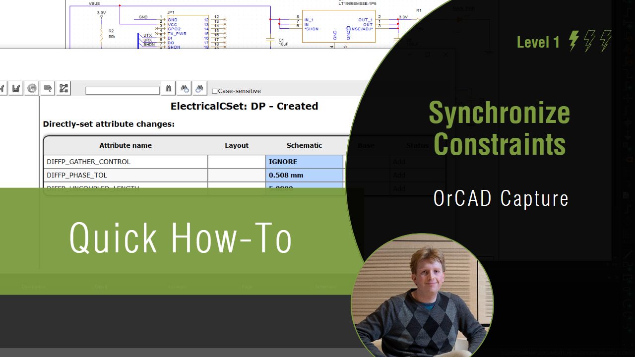
For a PCB design to be manufacturable and function as intended, it’s critical to meet certain design parameters and specifications. These specifications can be defined in either the schematic or PCB but must be communicated seamlessly for a successful design. OrCAD Capture and PCB Designer make it easy to synchronize constraints by defining and communicating design rules between the schematic design and PCB layout, keeping all stakeholders informed and the design in sync.
This quick how-to will provide step-by-step instructions on how to synchronize constraints with the Constraint Manager in OrCAD Capture and PCB Designer.
To follow along, download the provided design above the table of contents.
How-To Video
Updating the Design Layout
Note: This how-to will utilize Capture and PCB Designer together. If you have multiple monitors, configure Capture in one monitor and PCB Designer in another.
Step 1: Open the provided design, constraint_sync_tutorial.dsn,in OrCAD Capture.
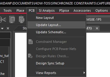
Step 2: Select PCB > Update Layout from the menu.
Step 3: Select Sync to open PCB Designer.
Note: This will enable a constraint driven design flow and sync the designs.
Step 4: Select the desired version of OrCAD PCB Designer from the software selection window.
Defining Physical Constraints
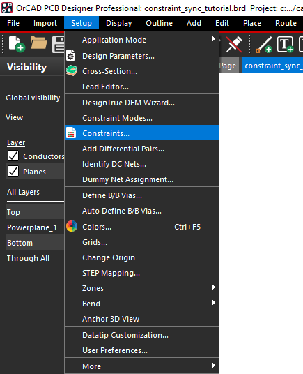
Step 5: In OrCAD PCB, select Setup > Constraints from the menu or the Constraint Manager icon from the toolbar.
Step 6: Select the Physical domain from the Worksheet Selector.
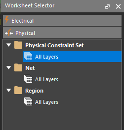
Step 7: Select the worksheet under Physical Constraint Set > All Layers.
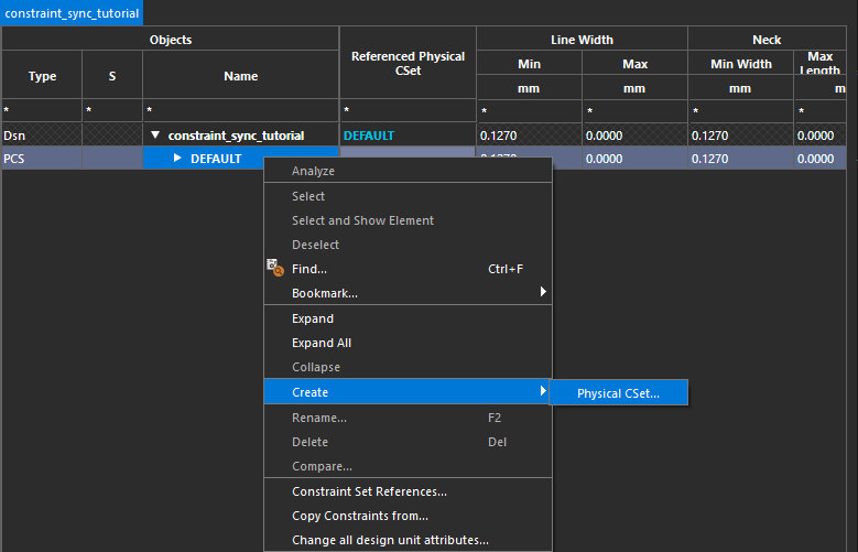
Step 8: Right-click the DEFAULT constraint set and select Create > Physical CSet.
Step 9: Enter DP for the name and click OK.
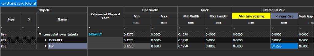
Step 10: Enter the following constraint values for the new CSet under their respective columns.
- Minimum line width: 0.127
- Primary Gap: 0.127
Assigning Physical Constraints
Step 11: Select the Net > All Layers worksheet in the Physical domain.
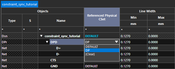
Step 12: Select the DP CSet from the dropdown in the Referenced Physical CSet column for DPD.
Note: Assigning this CSet at the top level will assign it to each net of the differential pair. For help with configuring differential pairs in the PCB, view our how-to here.
Step 13: Close the Constraint Manager.
Step 14: Select File > Save from the menu or the Save button from the toolbar.
Viewing Constraints in Capture
Step 15: Back in OrCAD Capture, select PCB > Update Schematic from the menu.
Step 16: The Update Schematic window opens. Select Sync.
Step 17: Select PCB > Constraint Manager from the menu.
Step 18: The Enable Constraint Manager window opens. Click OK.
Note: A window may open to assign voltages to power nets as well. Click OK in this window.
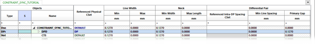
Step 19: The Constraint Manager opens. The physical constraints assigned in PCB Designer are shown.
Defining Electrical Constraints in Capture
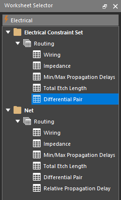
Step 20: Select the Electrical domain from the Worksheet Selector.
Note: Electrical constraints are available in OrCAD PCB Designer Professional.
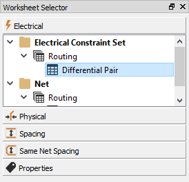
Step 21: Select the worksheet under Electrical Constraint Set > Routing > Differential Pair.
Note: For help with configuring differential pairs during the schematic design, view our how-to here.
Step 22: Right-click in the Name column and select Create > Electrical CSet.
Step 23: Name the CSet DP and click OK.
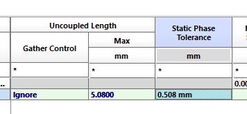
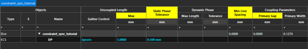
Step 24: Enter the following constraint values for the new CSet under their respective columns:
- Gather Control: Ignore
- Uncoupled Length: 5.08
- Static Phase Tolerance: 0.508
Step 25: Select the Net > Routing > Differential Pair worksheet.
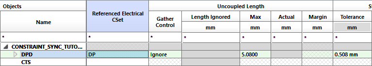
Step 26: Select the DP CSet from the dropdown in the Referenced Electrical Cset column for DPD.
Step 27: Close the Constraint Manager.
Syncing the Schematic and PCB
Step 28: Select PCB > Update Layout from the menu.
Step 29: Select Sync.
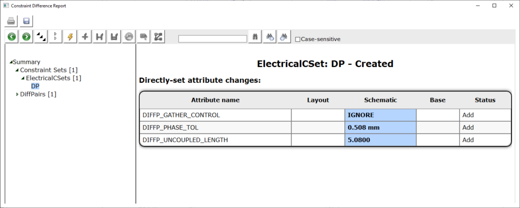
Step 30: A Constraint Difference Report is generated and opened. Expand and select Summary > Constraint Sets > Electrical CSets > DP. View the added properties.
Note: This report can be saved or printed to be viewed later.
Step 31: Close the Constraint Difference Report.
Verifying the Changes
Step 32: Back in OrCAD PCB Designer, select Setup > Constraints from the menu.
Step 33: The Constraint Manager opens. Select the Electrical domain and the Electrical Constraint Set > Routing > Differential Pair worksheet.
Step 34: View the defined table. The constraints have been imported from Capture.
Wrap Up and Next Steps
Ensure design intent and critical rules are accurately communicated between the schematic and PCB design with seamless synchronization of constraints in OrCAD Capture and PCB Designer. Test out this feature and more with a free trial of OrCAD.
