An XNet or extended net is a combination of a net, series passive discrete device(s), and another net between two pins. To define constraints for XNets and to perform an accurate signal integrity analysis, XNets must first be defined within the PCB.
This how-to will provide step-by-step instructions on how to setup Xnets in your PCB designs with OrCAD Capture and OrCAD PCB Designer Professional.
How-To Video
Editing Parts in the Schematic
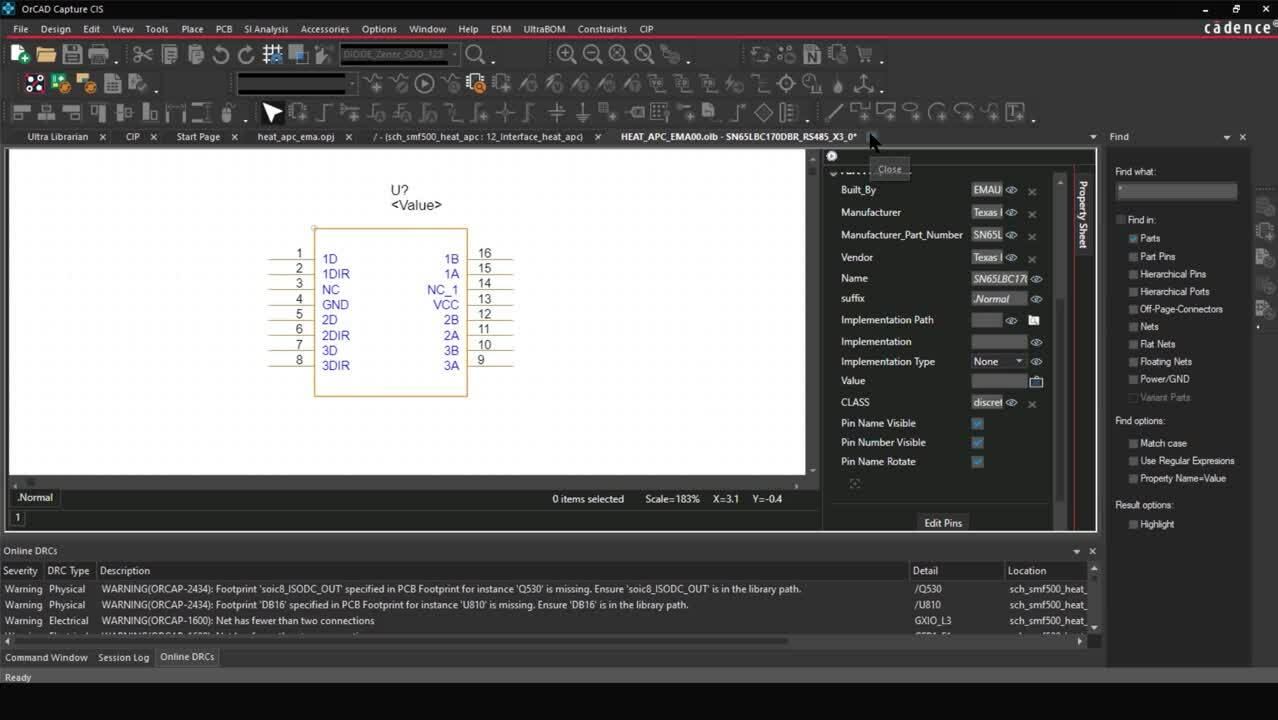
Step 1: Open the desired schematic in OrCAD Capture.
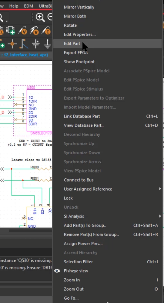
Step 2: Select the desired IC, right-click and select Edit Part.
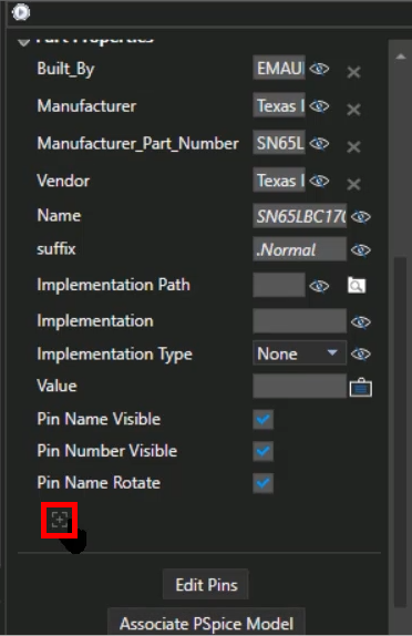
Step 3: Select the Add New Property button.
Step 4: Click the arrow and select Class from the drop-down menu.
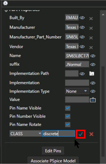
Step 5: Type Discrete as the class and select the check mark to add the property.
Note: Classes can be defined as IO, Discrete, or IC. For XNet creation, ICs must be changed to discrete.
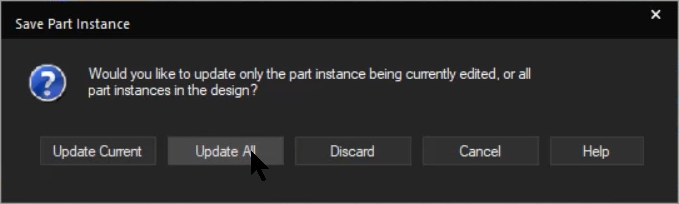
Step 6: Close the property window. In the Save Part Instance prompt, select Update All.
Step 7: Click Yes to save the design.
Configuring XNets in the PCB
Step 8: Open the PCB design in OrCAD PCB Designer Professional.
Note: To push changes from the schematic to PCB, select PCB > Update Layout from the menu. Click OK to synchronize the schematic and PCB design.
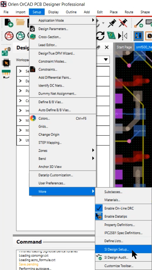
Step 9: Select Setup > More > SI Design Setup from the menu.
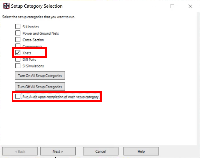
Step 10: Select only XNets as the setup category to run.
Step 11: If selected, deselect Run audit upon completion of each setup category.
Step 12: Select Next.
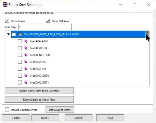
Step 13: Expand the design to view all the nets and deselect the box next to the design to clear the net selection.
Step 14: Select the desired nets from the list and click Next.
Step 15: Complete the steps outlined by the SI Design Setup Wizard.
Wrap Up & Next Steps
Quickly define Xnets in the PCB to assign rules and ensure signal integrity with the SI Design Setup Wizard in OrCAD PCB Designer. Try out these features and more with a free trial of OrCAD.
