IPC compliant schematic symbols should be used throughout the PCB design process to:
- Achieve standardization across all designs
- Improve clarity and understanding for all team members
- Increase efficiency in the design process
- Improve quality and reliability of the end product
- Adhere to regulatory compliance
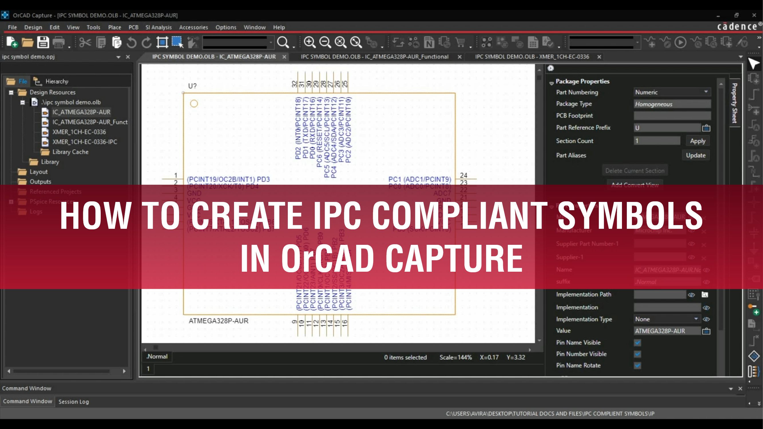
IPC compliance schematic symbols can be easily created in OrCAD Capture and used throughout your schematic designs. This video will provide an overview of industry standards to guide your symbol creation including :
- IPC-2612
- IEC 60617
IEEE/ANSI 315
Throughout this video, you will learn about the symbol creation process in OrCAD Capture and how to create an IPC compliance schematic symbol for a 32-Pin Atmega 328P from scratch using IPC-2612.
To follow along with the demo files, click here.