One of exciting things about the PCB design space is the pace at which things change and evolve. We are responsible for creating the tools that enable the design of the next great gadget or product. This puts us at the forefront of technology providing a “sneak peak” into future trends.
Below are a few trends we saw this year and ways we are trying to help our customers address them.
Flex is Mainstream
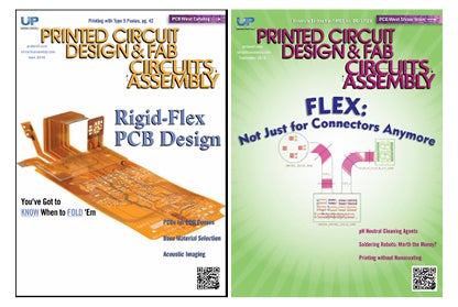
Flex and rigid-flex was a major theme this year (and into next). While flex technology has been around for a while, it seemed its use started to hit the mainstream in 2016. There have been many articles and editorials on flex over the course of the year. PCD&F even devoted 2 covers to flex in 2016.
Design teams are using flex for its well documented design benefits. These include: better space management, increased reliability, better signal quality, etc. However, along with these benefits come unique design and manufacturing concerns.
Unique Flex Support in 17.2-2016 Release
Cadence has long provided flex support. With the latest 17.2-2016, Cadence has made Flex a true first-class citizen in OrCAD and Allegro. Specific design rules and capabilities have been added to enable efficient flex based PCB’s while avoiding manufacturing or design issues.
Learn more about flex in OrCAD & Allegro:
Collaboration (People, Data, and Tools)
Collaboration is a key theme across businesses and business service providers. We have seen the rise of Slack for interoffice communications (and the later releases by Facebook and Microsoft of their own team collaboration apps). Having an API to hook tor connect your product with others is almost a requirement these days. There are even companies built solely around helping to stitch systems and data together like IFFFT or Zapier.
All these offerings center around the need to process information from multiple sources faster, with greater accuracy, and in context. PCB designers and engineers play a key role in creating the data processing and collection capabilities needed to support these data analysis platforms. This begs the question, what is being done to automate the design process for designers to keep pace with demand and produce the next generation of connected electronics?
It’s not a technology problem it’s a data problem
Many times the limiting factor for a company to achieve their PCB design goals is about process and data. Engineers have the skills and knowledge, but they are limited by their ability to access information, track changes, and effectively communicate with other stakeholders in the development process such as procurement, manufacturing, mechanical, other engineers, etc.
Engineers must log into separate systems or leave their design environments so they can stay in sync. While this may have worked in the past, the pace and complexity of development is demanding a “smarter” solution. One which empowers engineers with the data they need to make effective and timely decisions without burdening them. What design teams are looking for is a way to be “connected” without leaving their native design environment.

Context aware data management & collaboration
Cadence & EMA have released solutions in the past 2 years to help designs teams achieve this goal. From design data management and real-time collaborative PCB design to built-in PLM connectors, we are working to provide design teams access to the data they need while helping them maintain focus on the task at hand—building great products.
As we move forward, this need for integration and collaboration will continue to build as the design process becomes more interrelated and interdependent.
Learn more about our data management & collaboration solutions:
Supply Chain Starts at Part Selection
Another reoccurring theme for 2016 was companies looking to better manage their part supply chain. How do they specify the right parts the first time, thus avoiding late stage design revisions due to obsolete or out of stock parts?
Traditionally, engineers have had little visibility and influence into the supply chain. Part research was about finding a part that fit the design characteristics needed for the project. Little attention was given to cost, supply, second sourcing, and compliance (nor was this info readily available). Once the design is done, the BOM was something to send over the wall and let procurement handle it from there. Yet, as market windows shrink and PCB manufacturing has gone global, managing the supply chain upfront has become a strong interest for design teams to avoid late stage design changes.
To help design teams make supply chain driven part decisions, the new CIP Compliance Module was introduced which provides compliance data inside the PCB design environment. This system leverages SiliconExpert supply chain data (used by many in procurement and component engineering). Now design engineers and those managing the ultimate part purchases can work from the same dataset to verify the part will not only meet the electrical needs of the design, but can be ordered, and at a cost that will keep the product on budget and on schedule for release.
Learn more about Supply Chain Driven Design with OrCAD & Allegro:
2016 has been an exciting year for PCB design. Looking forward to what 2017 will bring.