A Directed Group is a component-based selection of nets, allowing you to select an entire interface based on component connectivity rather than net name. By using a Directed Group in your analysis, you can view the results for a collection of nets progressing along the same time-line. This helps you prioritize issues in your design; for example, issues found near the starting point versus issues found near the ending point. Focus your attention on known problem areas by performing the analysis on a portion of the net (between two desired components) rather than simulating the entire net.
Note: Directed groups can be used in both the impedance and coupling workflows.
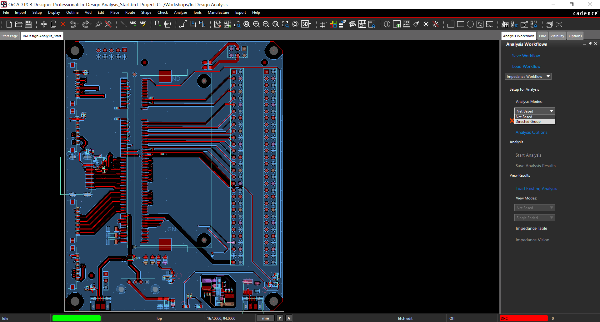
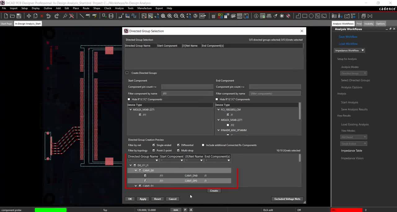
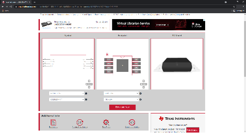
Step 1: With Impedance workflow selected, set the Analysis Mode to “Directed Groups” and click Select Directed Groups. This will bring up the dialog box to select, create or modify directed groups.
Note: The following information is included in the Directed Group Selection Dialog Box:
- Directed Group Selection: Lists the selected directed groups-the portion of a net between a starting component and ending component(s).
- Create Directed Group: Contains an expandable section to create directed groups by selecting the Start and End Component(s).
- Directed Group Creation Preview: Allows you to see a preview of the created directed group and select the desired nets.
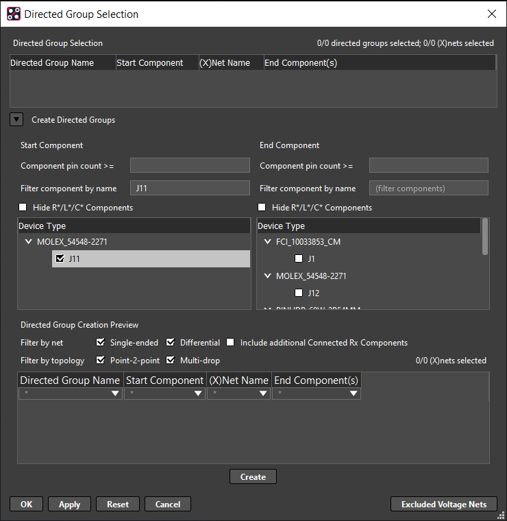
Step 2: Create a Directed Group. Select a starting component, J11, from the list in the Start Component section.
This will automatically create a list of the valid ending components in the End Component section.
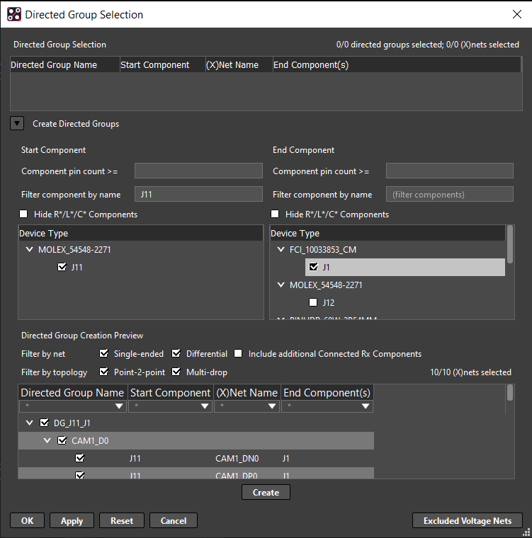
Select an ending component, J1, from the list in the End Component section.
Note: For boards with many components, filters are available to help find the desired components. Filter by pin count or component name. You also have the option to hide passive components (Resistors, Capacitors and Inductors).
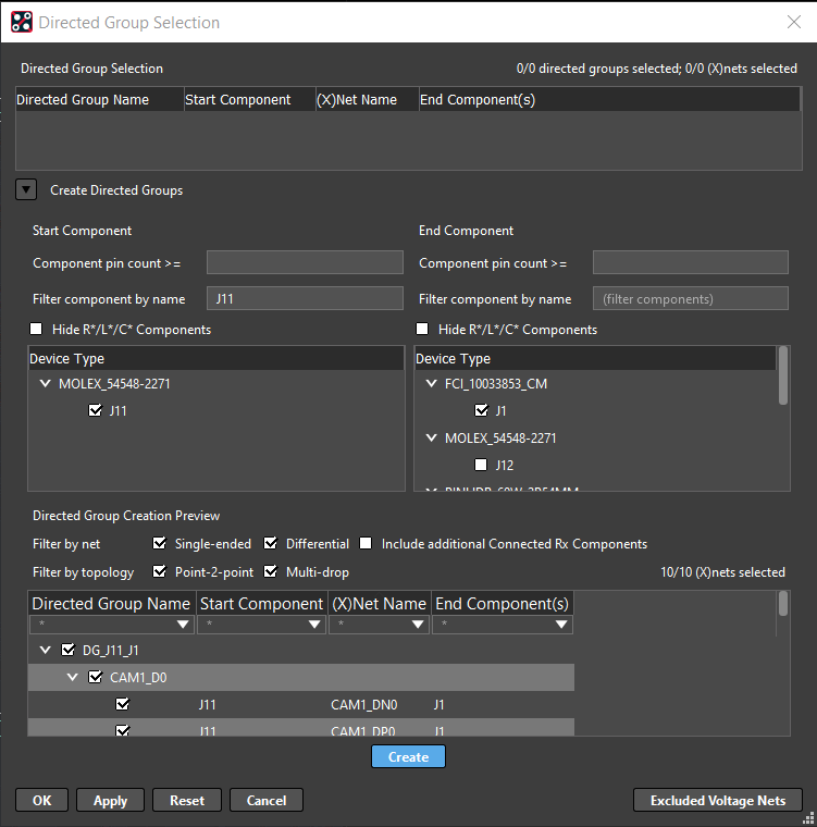
Step 3: Preview and Create the Directed Group.
Select the desired nets, DG_J11_J1, in the Directed Group Creation Preview window. By default, this is selected.
Note: You can filter by type of net (Single Ended or Differential) as well as topology (point-to-point or multi-drop) to find the desired nets.
Select Create. The Directed Group is created and can be viewed in the Directed Group Selection Window.
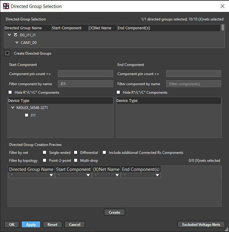
Note: By default, the created directed group is automatically selected for analysis.
Click Apply and click OK.
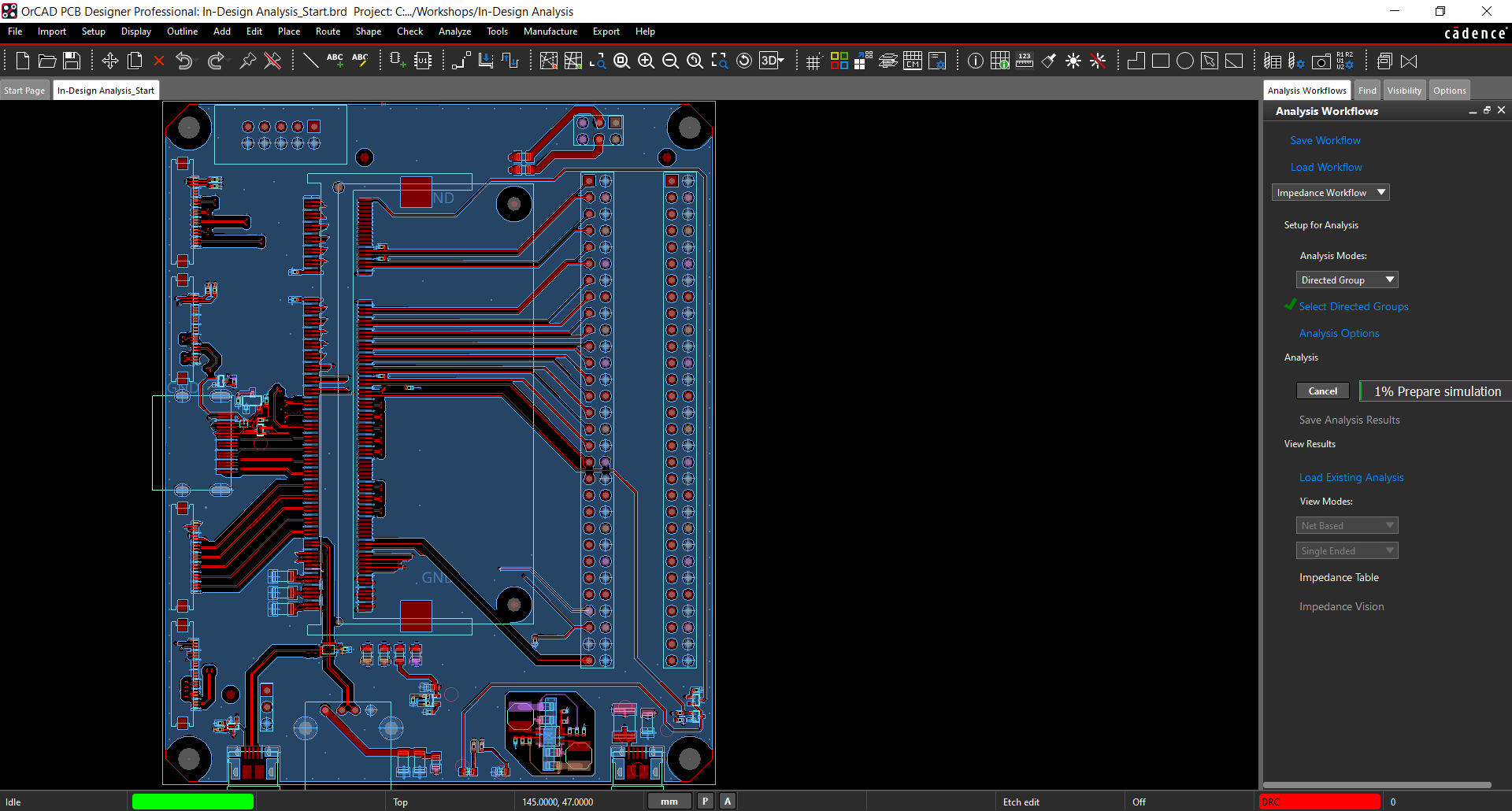
Step 4: Continue with the Analysis. Click Start Analysis in the Workflow Manager.
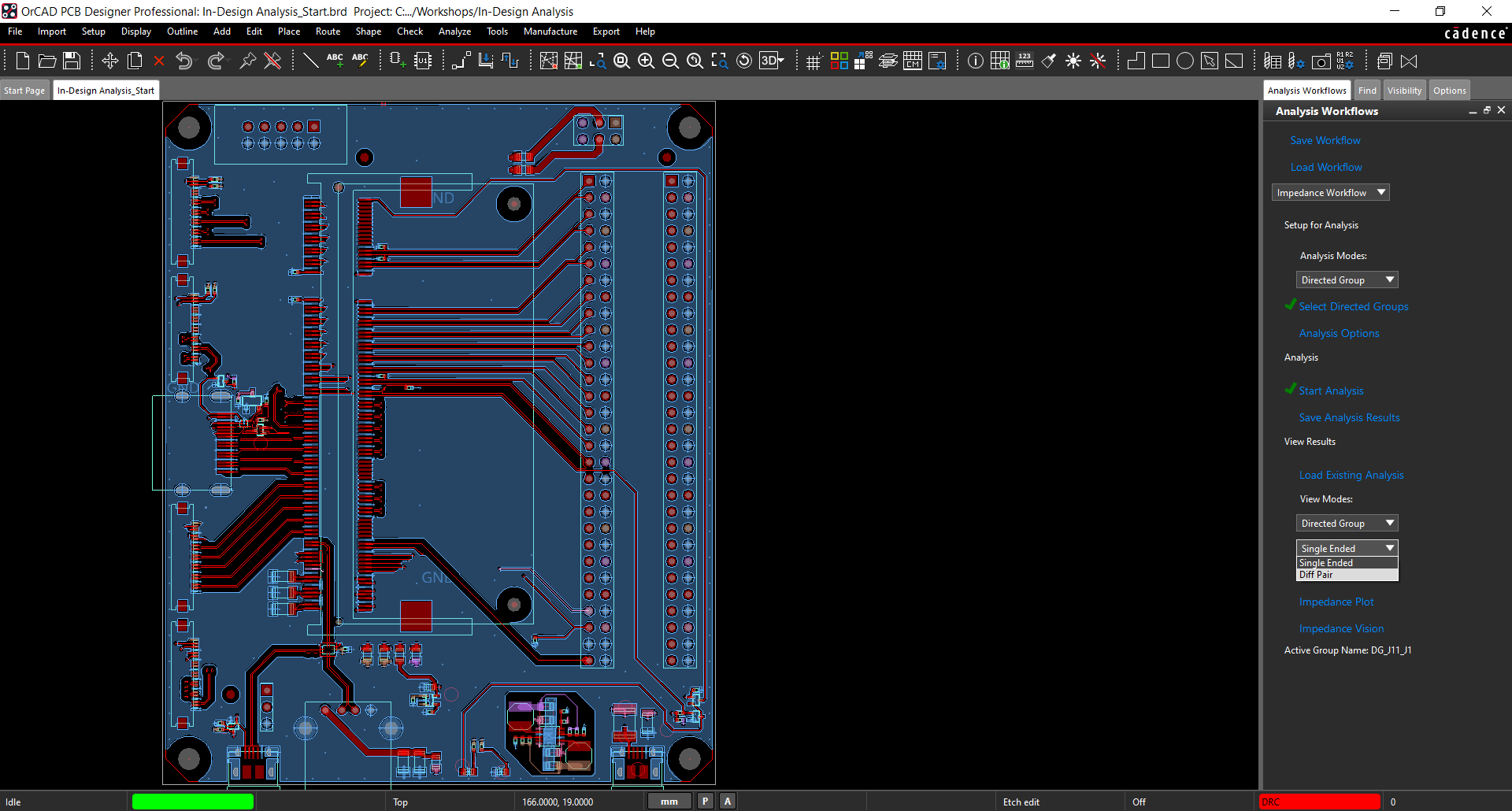
Step 5: View the results for the Directed Group. Under View Modes select “Directed Group” and “Differential Pairs”.
Note: This will generate the Impedance Plot or Coupling Plot (based on which analysis you are performing). It is important to note that this view is only available when performing analysis on Directed Groups.
Step 6: Click on the Impedance Plot to view the results.
View specific nets by using the selection window on the left or view simulation results for all nets in the directed group. By default, all nets are selected.
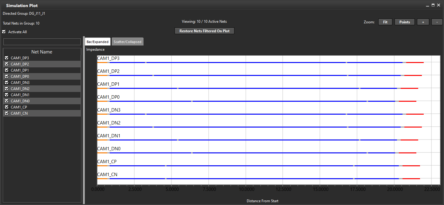
Select Bar/Expandable. Double-clicking on a portion of a net in the Bar Graph will bring you to the location on the PCB.
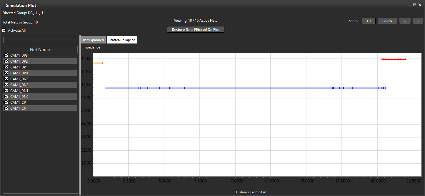
Select Scatter/Collapsed. This displays a global view which can be used to easily identify outliers.
Note: If results are not visible in the plot, select Restore Nets Filtered on Plot or Zoom Fit.
Video Tutorial: