Flex designs are becoming increasingly popular nowadays. The reason for this is because they not only save space and tend to be more lightweight (think cellphones and tablets), but when considered as part of the overall manufacturing and assembly costs, they can also reduce packaging complexity; improve product reliability; and reduce cost. Below are some General info on PCB and Flex Circuits as well as our Top 10 Tips for Flex Designs.
General Information on PCB and Flex Circuits.
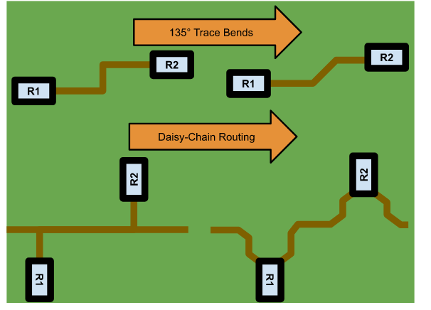
A. If the application requires bending in its daily operation no 90 or 45-degree bends or vias shall be used in the bend area. This sharp copper edge will cut the base material, normally a polyimide.
B. The flex circuit needs a cover applied and some call this a “cover coat” or “coverlay” opening in the coverlay for soldering of through hole and SM are needed.
C. The flex design should have stiffeners used at the components. If a Rigid Flex is being designed most parts are found on the rigid section so the need for a stiffener no longer applies.
Design considerations:
1. Plating materials: Solder, hard gold, soft gold, tin, nickel, silver, electroless nickel with immersion gold (ENIG), electroless nickel/palladium immersion gold (ENEPIG), organic solderability preservative (OSP) can be allied to the flex circuit.
2. Minimum width and spacing is .0015” or 0.038 mm, but it is not always good to hit the limits (plus it comes with a cost). Aspect ratio (ratio of hole depth/hole diameter) 12:1 maximum.
3. Control impedance for diff pairs on flex circuits are not a problem, work with your fab shop to get proper stack-up and width and gap for the diff pairs.
4. To increase flexibility, conductors should be staggered from layer to layer and not stacked on top of each other. Conductors should always be routed as close to perpendicular as possible through bend areas. Conductor thickness and width should remain constant in bend areas.
5. If the circuit will be bent within 1″ (25.4mm) of termination pads, fillets should be placed at each conductor/pad interface. Stresses from a bend are not isolated to the immediate bend area and residual stresses can radiate out from the bend area. Plated through-holes and vias should be kept out of the bend areas. Pad fillets improve etched yield and material strength. Fillets are appropriate when the pad diameter is greater than the connecting strand width. Acute angles at the interface between conductors and pads are to be avoided by using fillets to minimize the concentration of stress at the interface. Blind and buried vias and also tented vias can be used in flex designs.
6. If shields and/or ground planes are required on the circuit, use a cross-hatched pattern rather than solid copper.
7. Avoid any discontinuities in the coverlay or substrate near a bend.
8. Incorporate tear stops or reliefs for slits in the circuit (relief slots with 90 degree cuts). The end of the slit represents a vulnerable point for a tear to start and to propagate.
9. Stiffeners are created from a number of materials examples Epoxy-glass (FR-4), polyimide-glass, polyimide, copper, aluminum. Stiffener holes should be .015” or 0.38mm larger than the access hole on the coverlay.
10. Etched markings are allowed, Silkscreen marking can be applied, keeping out of the area of stiffeners.