Noise, which is best described as the presence of electrical energy where it should not be, is always bad. This is true whether it manifests itself in your ears as incomprehensible conversation or on a display screen as a collection of multi-colored pixels. Excessive noise can also disrupt circuit operation, which can cause severe outcomes in critical systems; such as medical devices, automotives, and aerospace systems.
Although noise may occur at any frequency, it is a much greater concern for high-frequency RF or when designing high-speed digital circuits. A major problem is when signals on adjacent/nearby traces interfere with each other due to electromagnetic coupling. Avoiding this common issue requires knowing and instituting good crosstalk reduction methods into your PCB design process.
Best Techniques for Minimizing Crosstalk
Crosstalk occurs when two transmission lines are close enough that inductive and capacitive coupling occurs. This is common in electrical circuits. For electronics, the objective is to minimize this interference by utilizing effective cross reduction methods, as shown in the table below.
All of the crosstalk reduction methods listed above are important and should be implemented, if possible. However, the most critical is to ensure there is sufficient spacing between traces. Following the 3W rule results in roughly 70% reduction in crosstalk. If 10W spacing is possible, up to 98% crosswalk resolution may be achieved. Although, rules of thumb can be helpful, implementing them well can be challenging, time-consuming and result in overdesigning. The most efficient and effective solution to mitigate crosstalk is to employ simulation targeted to the specifications of your design and implementation.
Implementing Crosstalk Reduction Techniques in Your Design
Reducing crosstalk is one of the most important signal integrity (SI) design challenges that engineers and PCBA designers must overcome to ensure reliable TX/RX for PCB design. As shown above there are methods to help in minimizing crosstalk and its negative effects. These are best implemented by following crosstalk reduction guidelines, as listed below.
PCBA Design Crosstalk Reduction Guidelines
- Understanding the causes of effects of crosstalk
Reducing crosstalk begins with clearly understanding that signal interference can occur between any traces in close proximity to each other. This is true for signals on different planes in multilayer PCB designs. And the results can range from signal variations and timing issues to erroneous circuit behavior. - Knowing the benefits of different crosstalk reduction methods
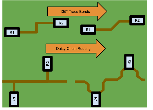
Different reduction methods have different effects on crosstalk. For example, minimizing trace lengths and widths reduce the amount of crosstalk that can occur. - Leveraging PCBA design software capabilities to institute reduction methods into your design process
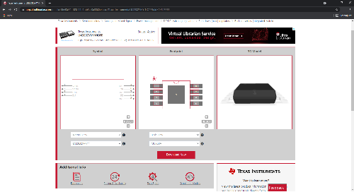
Most PCB design software tools will perform basic board design functions; including allowing you to specify design constraints. However, PCB CAD tools are not created equally and advanced capabilities to help you design for crosstalk reduction vary. - Employing simulation software to optimize SI for your design
The best way to ensure that your design satisfactorily minimizes crosstalk is to perform simulation, which is not included with most design programs. However, with the right PCB design and simulation software tool you can optimize your signals for serial TX/RX signal routing and across interfaces; such as for DDR implementation designs, and achieve the best crosstalk reduction.
EMA Design Automation is a leading provider of the resources that engineers rely on to accelerate innovation. We provide solutions that include PCB design and analysis packages, custom integration software, and engineering expertise, which enable you to create more efficiently. For more information on crosstalk reduction methods and how we can help you or your team innovate faster, contact us.