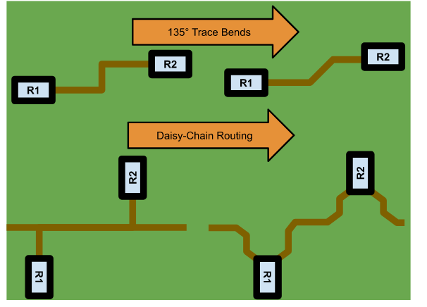
The process of designing electronic circuit boards in most cases is complex. To be efficient, engineers and designers must consider all three stages of PCBA development: design, manufacturing and testing. For example, when laying out the board choosing the best placement for components, traces and other conductive elements must be guided by DFM and DFA rules for manufacturing. Equally important is adhering to compliance testing requirements when required; like for reliable internal and external communication between USB devices.
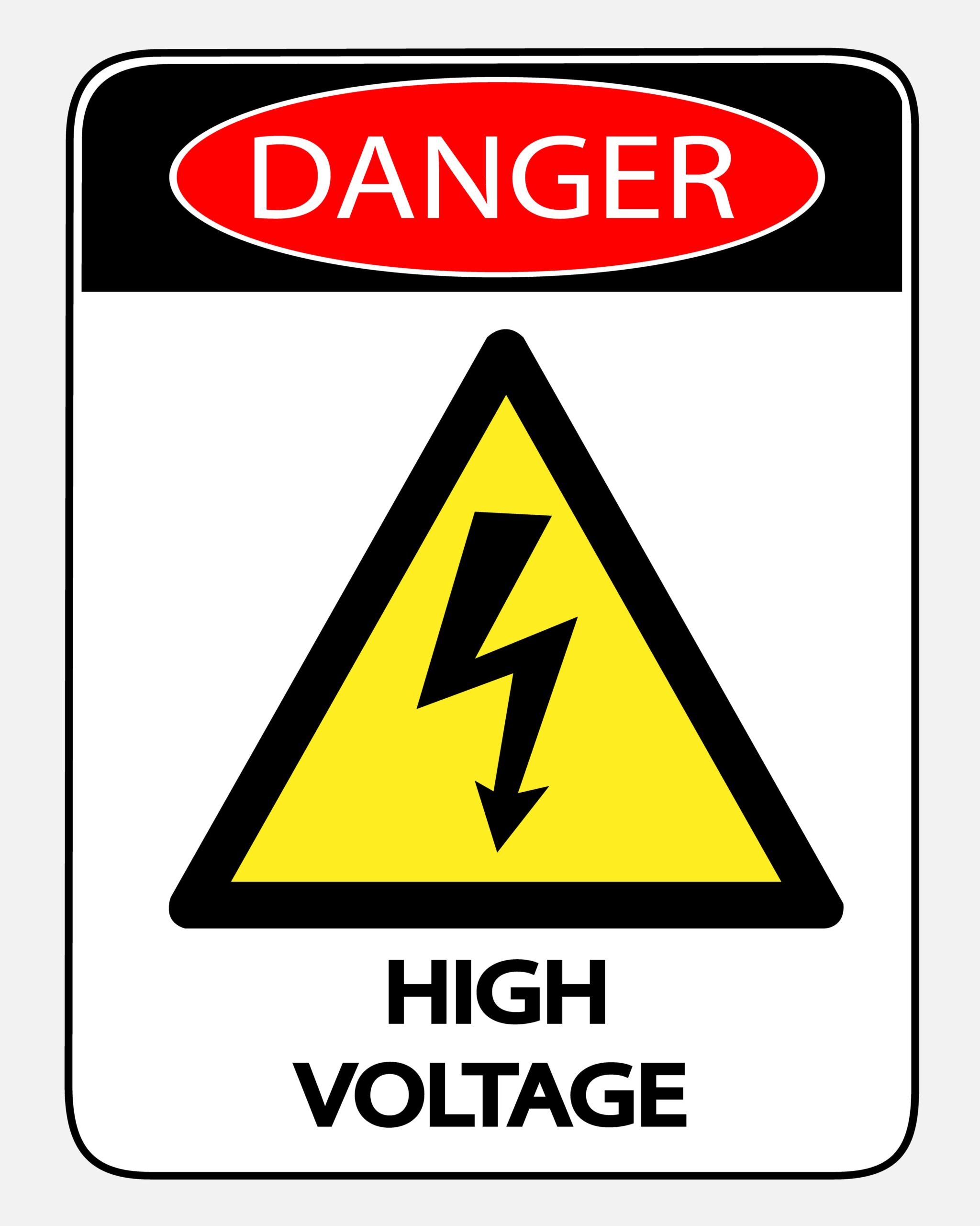
For high-voltage boards, safety must be added to the primary design considerations. High voltage TX/RX and/or high-power elements can create or attract currents at levels that can damage components, the board itself or even threaten nearby users. To combat these contingencies, there are specific PCB standards that define acceptable spacing between conductive elements. Knowing and following these PCB clearance and creepage distance table specifications is essential when designing high-voltage circuit boards.
Important Clearance and Creepage Distance Requirements
Not surprisingly, there are several industry standards that include specifications meant to ensure that PCBs and electronic devices are safe. Among these are IPC-2221, IPC-9592, IEC-6061 and IEC-62368. Each of these provides guidance and direction for placing components at distances to minimize the possibility of hazards; such as shorts and surface tracking. The most implemented of these are shown in the clearance and creepage distance tables below.
PCB Clearance Distance Table
For clearances, IPC-2221B is the prevailing standard and includes the specifications listed below.
The clearance distances above apply to conductors with the following attributes:
- B1 internal conductors
- B2 uncoated external conductors, up to 3050 m above sea level
- B3 uncoated external conductors, higher than 3050 m above sea level
- B4 polymer coated external conductors, at any elevation
- A5 conformal coated external conductors, at any elevation
- A6 uncoated external component leads/termination, up to 3050 m above sea level
- A7 conformal coated external component lead termination, at any elevation
PCB Creepage Distance Table
For creepage distances, IEC 60950-1 served as the industry standard for decades. However, many countries have adopted the more robust IEC 62368-1 for new product development. The intent of maximizing safety for users of electrical/electronic systems, especially for high-voltage applications, remains the primary objective and is reflected in the specifications below.
As illustrated in the table above, the minimum creepage distances are classified according to pollution degree and material group for various RMS voltage levels. The degrees for pollution are divided into three groups based on the amount of pollution or its conductive impact. Degree 1 indicates none or only non-conductive pollution, while degree 2 refers to pollution that is typically non-conductive that may gain conductivity as a result of condensation. An environment that is normally conductive is classified as degree 3. Materials are segregated into four groups, according to IEC 6064-1, according to the rated comparative tracking index (CTI) that quantifies a resistance to conductive tracking through the material.
Following Clearance and Creepage Distance Table Rules
Today, electronic circuit boards are used in virtually every class of product, appliance, system or platform. Consequently, safety should be a major consideration for any PCBA development process. This concern is elevated even higher for high-voltage boards. Therefore, it is critical that your PCB development tool(s) include functionality and capabilities intended to not only ensure performance and maximize efficiency, but also to incorporate safety standards and guidelines like the creepage and clearance distance rules discussed above.
EMA Design Automation is a leading provider of the resources that engineers rely on to accelerate innovation. We provide solutions that include PCB design and analysis packages, custom integration software, and engineering expertise, which enable you to create more efficiently. For more information on how to incorporate clearance and creepage distance table rules and how we can help you or your team innovate faster, contact us.