You may think if your devices are operating at lower frequencies then your board is not high-speed; this not the case. Any PCB where the quality of your signals is being affected by the PCB layout is a high-speed board design.
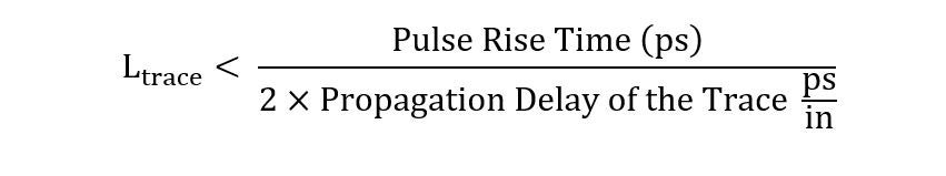
You determine this by checking the amount of time it takes for a chip to switch a digital signal from the ‘off’ to the ‘on’ state. Typically, if the signal pulse rise time is ‘small’ compared to the time it takes for the signal pulse to propagate (e.g. ½ of the total time the signal takes to travel along the trace) then you need to consider your PCB as a high-speed circuit, because the entire signal pulse will manifest on that trace before hitting the end of the trace. We can use an equation to understand this.
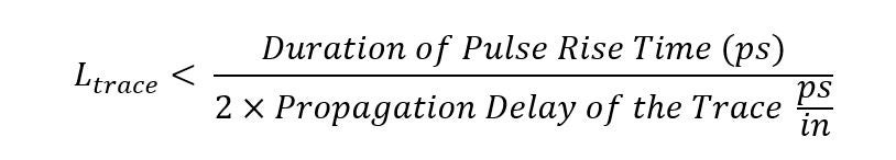
This expression is telling us if we don’t want to deal with a high-speed PCB trace (i.e. we do not want to have to treat the trace as a transmission line), then we need the length of the trace, Ltrace, to be shorter than the expression on the right.
What is the duration of the pulse rise time? This is the length of time it takes for the signal pulse to go from ‘0’ to ‘1’ or 0 to 3.3 V. Technically the pulse rise time would be measured as 10 % to 90% of its maximum value, but let’s go with 3.3 V for ease of calculation. Let’s assume this takes about 3 nanoseconds to get to 3.3 V, look at the propagation delay of the trace. This is how long it takes for the pulse itself to ‘travel’ from one end of the trace to the other end. The pulse could go extremely fast, like near the speed of light fast (84.7252802 × 10⁻¹² seconds in one inch), but every material has its own properties which would prevent that pulse from traveling as fast as light. We call this property, the propagation delay of that trace.
For instance, a signal pulse on a trace exposed to air or a vacuum travels at a speed of about 84-85 picoseconds per inch (about 11.8 inches per nanosecond). However, if that trace were immersed in common dielectric material, like FR4 Isola 370HR, the pulse would slow down and take 145 picoseconds to travel that same inch. Whichever material you’re working with, speak with your manufacturer to find its propagation delay. You can also consult the IPC-2141A however, manufacturers would have the latest information.
Now that we understand pulse rise time (0 to 3.3 V in 3 ns or 3000 ps) and propagation delay (~85 ps per inch), we can find out the longest we can make a trace without it becoming a transmission line.
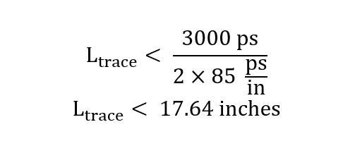
This means we need the trace to be under 17.64 inches on the surface of the PCB for this specific material to not be considered high-speed. In contrast, for an internal trace with the same dielectric material we need the trace to be less than 10.34 inches to not be considered high-speed.
If your chip pin (we call this the driving pin) turns its signal from ‘off’ to ‘on’ in 3 ns (3000 ps), and those signal pins are attached to a trace that is 17 inches or longer on your PCB, then you have a high-speed board.
Ideal Trace Length for a High-Speed Transmission Line
The values we calculated are near the ‘critical trace length’. Ideally for such fast signals, we do not want to be near this trace length as we can still be at risk for ringing and other issues. Therefore, a good rule of thumb is to design your trace such that it is 1/15th the wavelength of the signal (according to IPC-2251).
For analog signals the wavelength can be approximated to the signal propagation velocity through the trace in inches per picosecond (this is the inverse of the propagation delay), divided by the frequency of the signal (in Hz).
Applying this knowledge, we know 1/15th of 17.64 inches is 1.176 inches. Therefore, keeping the trace under 1.176 inches is ideal for digital signals.
For analog signals on that trace, less than 1/15th of the sinusoidal wavelength is ideal. The wavelength for this situation with the trace exposed to air comes to 35.4 inches.
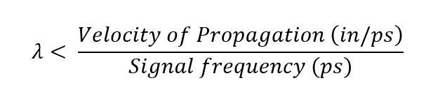
So, 1/15th of 35.4 inches is 2.36 inches for the recommended max trace length to avoid reflections.
For an exposed trace on FR4 dielectric material, a good rule of thumb is to design the trace to be 1/10th of 5 times the rise time, then slap the ‘inches’ unit at the end of it. For example, I should design a trace to be 1/10th of (5×3 ns) in. for a pulse that has 3 nanoseconds of rise time.
This equates to:


Why did I choose 1/10th instead of 1/15th? This is a quicker way to estimate trace length for practical routing to avoid signal reflections without having to use termination techniques. If we cannot make a trace that short, then we can reference the earlier equations to determine critical trace lengths and possibly avoid signal termination or transmission lines.
If I Have a Certain Chip or Crystal Frequency, Does That Make My Board High Speed?
Regardless of the frequency of any device on your PCB, like chip or crystal clock frequency, your PCB may or may not need to be treated as a high-speed board. You must check your signal rise times for your driving chips.
If any of those chips sends a signal with a fast enough rise time compared to the PCB trace length and at a fast enough frequency, your board can possibly fail EMI testing at a 500 kHz switching frequency or even 50 kHz, or 50 MHz, etc.
Signal Integrity is in Everyone’s Future
Identifying your board as ‘high-speed’ is no longer as simple as just looking at the frequency. Keeping chip speed in mind is essential. This will dictate your design requirements and allow you to make informed choices as you work to create reliable products and accommodate ever-evolving technology. As chips get faster rise times, unless you specifically choose older ‘slower’ ICs (not clock frequency, but pin-signal rise time), then signal integrity is in your future. This means if you don’t design for signal integrity now, the same board design might fail in the future as you start to incorporate newer part versions.