As products, vehicles, and appliances continue to get smarter, the demand for more advanced electronics and PCBAs continues to grow. However, the PCB industry is a highly competitive market. Therefore, it is important to ensure that your electronic circuit boards are reliable, meet performance objectives and that your development process optimizes quality and is efficient, fast, and cost-effective. The right professional product design software will help your engineering team(s) optimize the design, build, test (DBT) cycle and overcome development challenges.
Best Professional Product Design Software
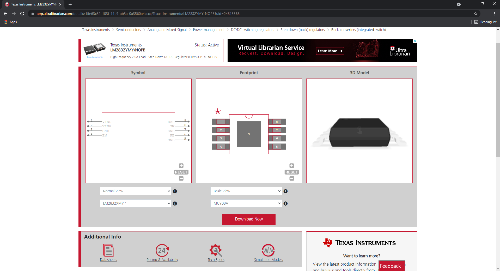
Although, there are many PCBA design programs available, the range of specialities and capabilities vary greatly. Below, a listing of the best professional product design software tools for different applications are listed.
The list above includes the best professional product design software tools for different aspects of circuit board design. Employing these tools individually or collectively will help you optimize your design and development process. Knowing what tools to incorporate into your process begins with understanding the development challenges for optimal PCBA design.
Electronics Product Development Challenges
For electronic circuit boards, new product introduction (NPI) consists of two similar yet distinct processes. These are development and production. Production, which may be low or high-volume, is typically a manufacturing-only stage, where maximizing yield rate and minimizing cost are the goals. The development process is more complex.
PCBA development is a three-stage iterative process comprising design, manufacturing, and testing. The overall development objective for all team members is to create a production-ready design that addresses the development challenges listed below.
Major PCBA Development Challenges
Maximizing Product Quality
Board quality is not directly calculable but can be readily determined. Your board’s ability to consistently function as designed and meet its performance criteria over its operational lifecycle defines its quality. Although your contract manufacturer (CM) is responsible for building your board, the quality of the manufacturing process and, therefore, the final product greatly depends on your utilization of DFMA rules and guidelines.Mitigating Supply Chain Issues
The most important design decisions you make for PCBA are what components to use. Part selection involves more than researching capabilities and choosing a package type today. The volatility in the electronics supply chain requires you to institute an effective library management solution that provides accurate data. Otherwise, your development schedule can be interrupted or halted due to the unavailability of the parts you need.Managing Costs
PCBA design is bounded by constraints. These include limitations on component functionality, your CM’s manufacturing equipment capabilities, enclosure size, or other installation environment parameters. In addition to these technical restraints, you must strive for cost-effectiveness as company profitability depends on managing development ROI.
Although your enterprise EDA software may provide options that help your team address one or more of these challenges, most are not designed to do so. For these cases, selecting the best professional product design software based on your specific needs is required to target and successful address these issues.
How Professional Product Design Software Solves PCB Development Issues
The most effective PCBA development is accomplished when each of the three DBT stages is optimized individually and performed to help facilitate the performance of the other stages. Manufacturing and testing are more rigid, and the equipment used is fixed. Therefore, the key driver of optimal development is the design. Many PCB design software programs allow for simultaneous or concurrent design engineering tasks to be performed across the team, yet are not directly designed to optimize development quality, efficiency, and costs. By incorporating software tools that integrate with and enhance your EDA program’s design capabilities can achieve this goal and deliver the following benefits.
Advantages of Choosing the Best Professional Product Design Software
★ Improves Product Quality
The best product and process quality are attained when your boards are designed for first-pass right board build. Real-time DFM checking gives the ability to make corrections and changes during design and verify manufacturability, thereby avoiding the typical back and forth between the design team and CM that slows the development process.★ Helps Avoid Supply Chain Issues
The integration of design and a library management solution helps to avoid supply chain issues like choosing parts that are out of stock, obsolescent, or even out of production. Further, sourcing from a comprehensive, reliable source can ensure that component schematic symbols, board footprints, 3D CAD models, and support data are accurate.
Learn more about how to avoid supply chain chaos.
★ Lowers Overall Cost
Most PCBA development costs are well-defined. For example, CM manufacturing costs are typically fixed unless there are special requirements. And for a large PCB layer count, complex via-in-pad construction, high Tg material usage, in-circuit tests (ICTs), and other non-typical specifications will increase the cost of your board build. In most cases; however, cost variability comes from the need for excessive respins due to design specifications and CM DFM or DFA misalignment. Using product design software tools that improve process quality, efficiency, and speed optimizes the use of engineering resources, which minimizes overall project costs.
Choosing the Best EDA Software Tool for Your Project
The need to optimize your development process will only continue to be more crucial to compete in the PCB industry. The best first step is to rely on a good PCBA design program as the foundation for your design process. This is followed closely by choosing the best EDA software support tool(s) for your project.
Best Professional Product Design Software Selection Tips
☐ Make sure the tool is compatible
The most important requirement for your design support tool is that it easily integrates with your enterprise PCBA design program. If you use one of the more advanced PCB design packages, functionality and capabilities like the ability to perform high-level RF analysis, may be included. However, if a third-party tool is required, there can be problems. These include file format conversions that can introduce errors or where important data can be lost.☐ Ensure the tool(s) performs the range of functionality required
It is also important that your choice of support tool is capable of performing the range of functions that may be required by your team(s). For example, it is common for PCBA design today to have RF radiators or other EMI/EMC concerns. A good support solution may require multiple tools. It may be necessary to combine these in order to address different specifications; such as design verification for manufacturability, circuit performance and operation. This will help avoid functionality testing failure that can require redesigns and respins.☐ Choose a tool that is well supported
Any software tool of any complexity comes with a learning curve before proficiency is attained. Therefore, adequate information and support should be available. If excessively long training periods are required, your use of a professional product design software tool can work to decrease the efficiency of your process.☐ Plan for the future
Another essential consideration for choosing a support tool is whether it is extensible and will grow as your design needs do. Whether driven by technological advancements, customer demands, and/or industry standards, board and product requirements will undoubtedly change, and you want to avoid having to relearn a tool for these inevitable evolutions.
The best way to satisfy these requirements and optimize your team’s product design process is to rely on an industry expert with a proven track record of developing solutions to help PCB designers create faster and more efficiently.
EMA Design Automation is a leading provider of the resources that engineers rely on to accelerate innovation. We provide solutions that include PCB design and analysis packages, custom integration software, and engineering expertise, which enable you to create more efficiently. For more information on professional product design software to help you or your team innovate faster, contact us.