As the applications for electronic circuit boards continue to expand, the demand for greater functionality in smaller products continues to increase. Evolutions in component manufacturing techniques and the range of materials used are the most significant advancements that enable these goals to be largely met. However, using these technological advancements requires improving how boards are designed and built. One of the important of these improvements is the implementation of multilayer PCB design guidelines.
Why Are Multilayer PCB Design Guidelines Important?
PCBs can be classified in many ways. For example, high-speed and power group boards according to usage or application. The most common categorization is based on the PCB stackup, as listed below.
Although the manufacturing process is similar for all board types listed above, there are additional steps for multilayer PCBs. The inclusion of internal layers requires designers to make decisions and specify board parameters, if and where to use via-in-pads, that are otherwise not necessary.
Important Guidelines for Multilayer PCB Board Design
It may not be intuitive; however, using multiple layers in your stackup affects virtually all aspects of the PCB design process. For example, spacing and clearance routing must now consider the angle of signal traces on adjacent (internal) layers. The most important multilayer PCB design guidelines to implement are described below.
The above list is not exhaustive. For example, it does not include impedance control which is a greater challenge for multilayer boards than for other designs. Yet, it does include important multilayer PCB design guidelines that should be followed to facilitate the optimal development of standard rigid circuit boards. For flex PCBs, there are additional issues to consider.
Additional Considerations For Flex PCB Design
The increased use of full and rigid-flex circuit boards is one of the major trends in the electronic products industry. This is due to mounting and installation flexibility, ability to withstand vibration, and increased thermal resistance. These are common in harsh environments like space, factories, and automotive systems. To realize these advantages requires consideration of the following:
Multilayer Flex PCB Design Guidelines
- Do not exceed bend ratio standards
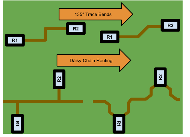
How far the board will need to bend compared to flex circuit thickness is the bend ratio. For flex boards, the ratio is 20:1 for PCBs that will remain static during operation. - Traces should be alternated on top and bottom
Stacking copper traces can lead to premature board degradation; therefore, staggering traces is recommended. - Only use through hole vias
Through hole vias are recommended for flex sections or boards as other types may result in loss of connection. - Use large annular rings for vias
Small annular rings may result in loss of connections between copper traces on separate layers. - For rigid-flex, place the flex area in the middle of the board
Being surrounded by rigid materials aids in maintaining structural integrity and long-term reliability of the board.
The multilayer PCB design guidelines above should be incorporated when designing rigid and flex boards. For most EDA programs, it will be necessary to edit or create constraints to ensure your DRC alerts you when there are errors. The best option may be to partner with an industry expert that can provide you with software tools and solutions that integrate with design software to help facilitate the most efficient development of your new product.
EMA Design Automation is a leading provider of the resources that engineers rely on to accelerate innovation. We provide solutions that include PCB design and analysis packages, custom integration software, and engineering expertise, which enable you to create more efficiently. For more information on important multilayer PCB design guidelines and how we can help you or your team innovate faster, contact us.