Does this situation sound familiar? You complete your design and send it off to the fabrication house only to have your product’s development cycle put on hold for numerous DFM (design for manufacturing) errors. Being in this situation can not only be frustrating, but also costly. Considering manufacturing issues early within your project timeline helps to lower costs and development time, and ensures a smooth transition into production. Not performing checks to verify that your design adequately addresses common PCB manufacturing problems, all but guarantees the opposite.
From conversations with customers and our years of industry involvement, we have compiled a list of the top DFM issues which prevent PCB manufacturability.
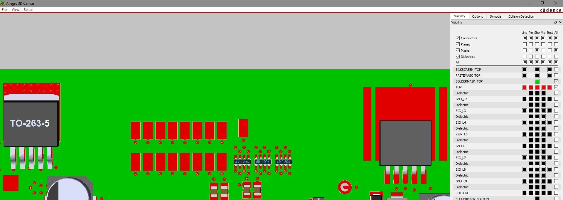
Important DFM Issues To Check
While consideration of some of the issues listed below can be considered PCB layout design best practices, others are defined by the fabrication/assembly house themselves through DFM and DFA (design for assembly) rules and guidelines—which are often included as part of DFM. By evaluating these issues in the design phase of your project, you will be able to correct any potential DFM issues before your board design file gets to your manufacturer’s shop.
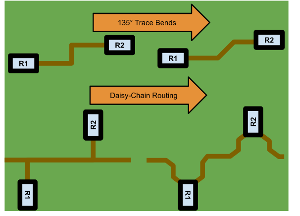
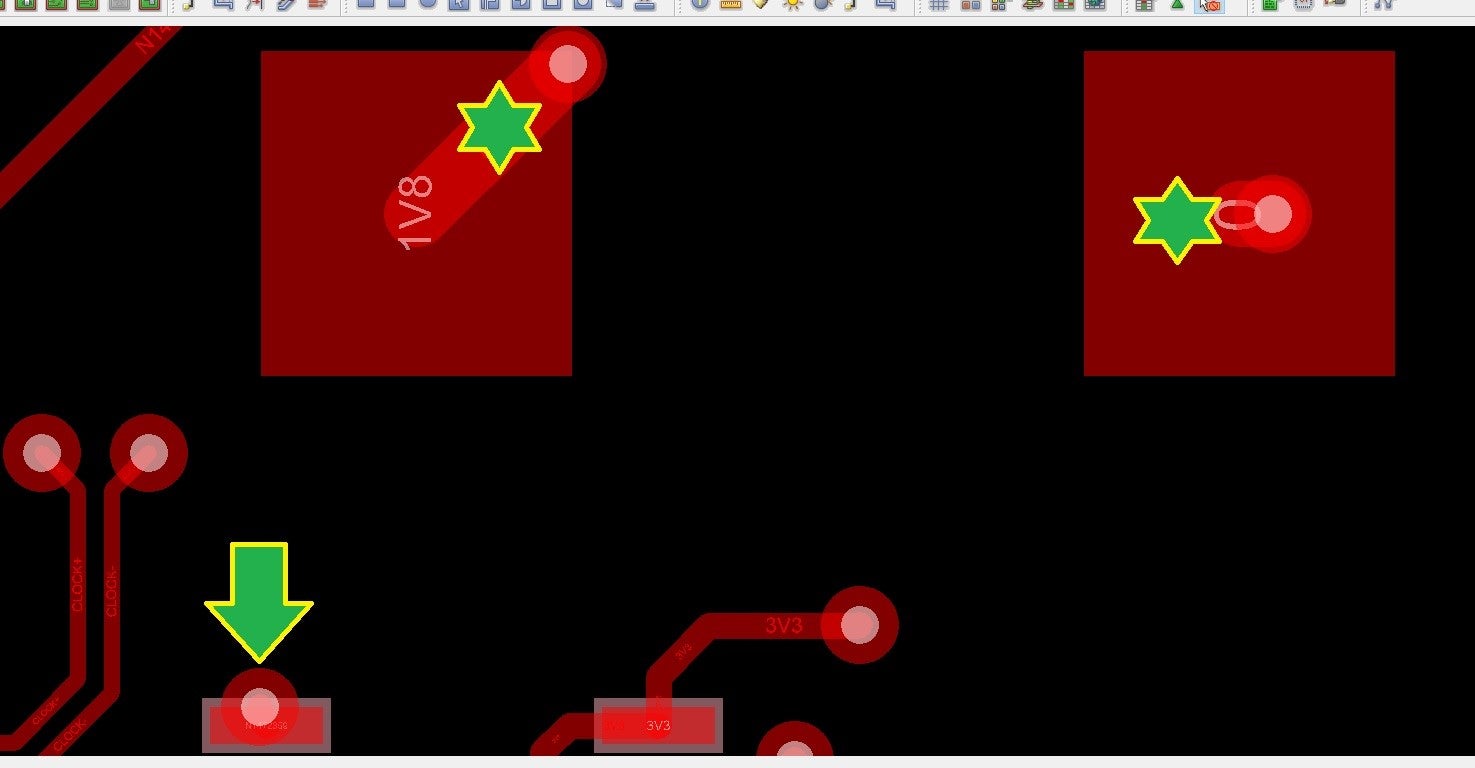
DFM Issue #1: Acid Traps
When we are discussing acid traps, we are describing acute or odd angles of copper features on the printed circuit board which cause acid to pool during the PCB creation process. An example of this issue is shown in the figure below.
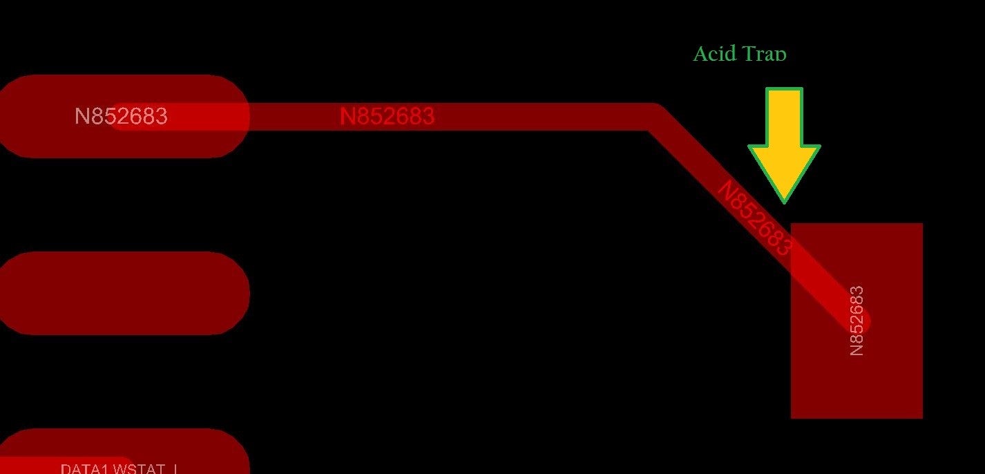
These acute or odd angles of copper become an issue before the wash process, allowing residual acid to get caught and not get cleared away. As a result, the wanted copper features the Gerber file included on the board begin to erode, creating “opens” or lost copper connections. This situation can be identified, provided your design software includes functionality as shown in the image below.
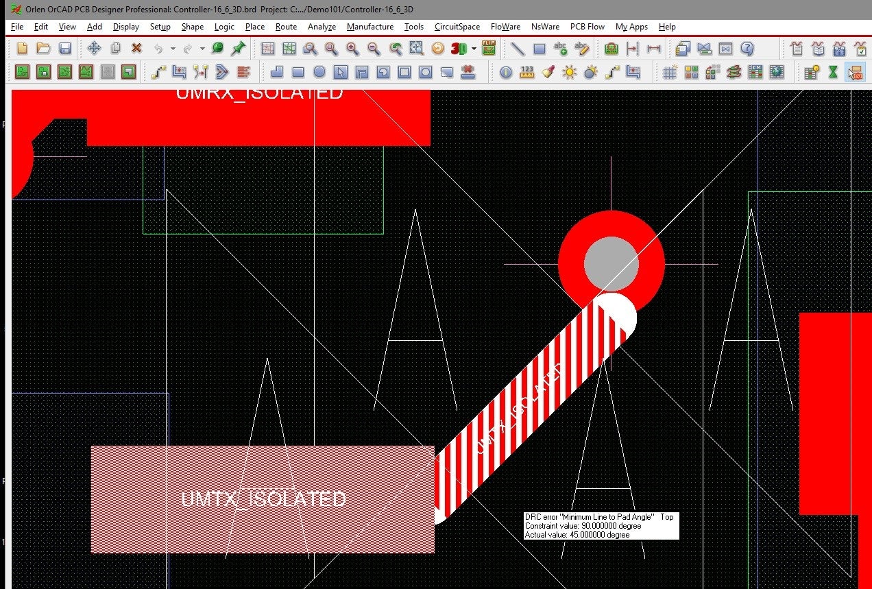
Avoiding acid traps are especially important with the 4 or 5 mil traces on today’s designs. Since they are so thin, they can easily become open (openings created within wanted copper due to trapped acid). Some ECAD software programs have the capability to check for these problems. If your PCB design program does not, you will have to manually evaluate the board to avoid creating designs that have this issue.
Note: To prevent acid traps, avoid placing the trace coming into a pad at an acute or odd angle. Keep angles 45° or 90° adjacent to the pad.
DFM Issue #2: Slivers and Islands
Slivers and islands are free-floating copper on many plane layers that can create some serious problems in the acid tank. The following images illustrate these issues.
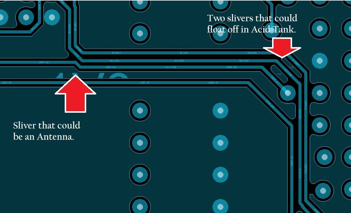
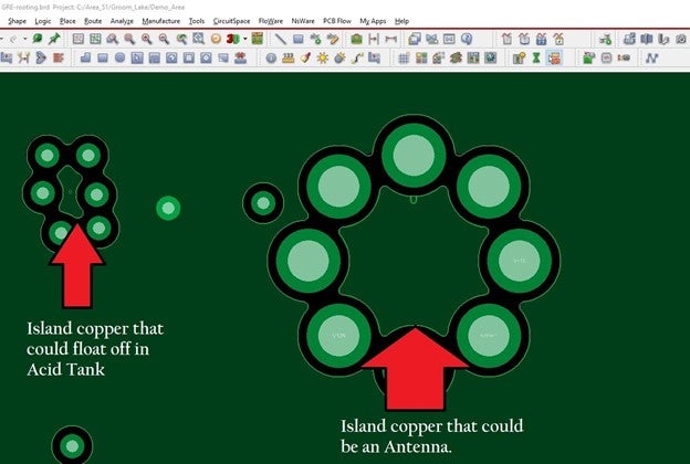
Several DFM issues can occur because of slivers and islands. The small specks of copper have been known to float off the PCB panel and find their way to other etch on the panel creating a short. Or, if they are large enough to not be able to float off, it becomes your antenna—which can cause noise and other interference within the board (because it's copper with nothing grounding it—it becomes a signal gatherer). As shown below, some software tools can search for these within your design.
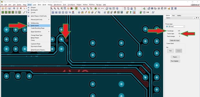
However, if your design program does not have this capability, you will have to manually find and remove slivers and islands from the board design.
DFM Issue #3: Solder Bridges
Solder bridges are unwanted connections between conductive elements of your board. A common occurrence is solder bridges forming between pins, which the figure below shows.
With etch traces being so fine-lined and pin-pitch so tight, it is essential to include solder masks within a PCB design. Excluding solder masks can result in a large blob of solder (especially between pins) during assembly–resulting in a short. In addition, it can also cause reduced corrosion protection on other copper on the outside layers. To help prevent these issues, be sure to check the alignment, solder mask to solder mask (webbing) spacing from pad to etch lines and to shapes. Also, be sure there is no solder mask covering pins.
Note: Your assembly house can inform you of the minimum webbing space and alignment they will allow.
DFM Issue #4: Paste Mask Openings
Heatsinks absorb and dissipate heat from an electronic component through contact with a metal base or thermal interface material. If the paste mask openings are too large in the heat sink, once the solder paste melts, it could cause components to float off the pads. This is illustrated below.
To prevent this, reduce how much paste is put down on a heat pad; instead of one large paste mask opening, try breaking it up into several, smaller paste mask openings. This will help ensure components will not float and crash into other parts during the reflow process, which can cause shorts. Paste mask openings are an essential part of DFM checks. Before sending off to manufacture, ask yourself: Do all the component leads on the PCB have the proper paste mask opening (and size) for the stencil?
Note: Your manufacturing engineer should be able to provide you with the size requirements of your paste mask opening.
DFM Issue #5: Via-in-Pad Alignment
When incorporating via-in-pads in your board design, care must be taken to make sure accurate alignment. Failing to do this may lead to cold solder joints or no solder connection, as shown in the PCB layout design below.
Checks for vias within pads are essential; if the via is not properly placed, it could allow solder paste to flow down into the via. This will result in a cold solder joint or no real solder connection. You need to find out what percentage of the via is allowed in the pad before plugging the via. It’s the hole in the via that creates the problem, not the pad. Most design programs should be capable of checking for these DFM issues. If yours does not, you will have to manually check your design to be sure it is in compliance with your assembly house criteria.
DFM Issue #6: Copper-to-Board Edge Clearance
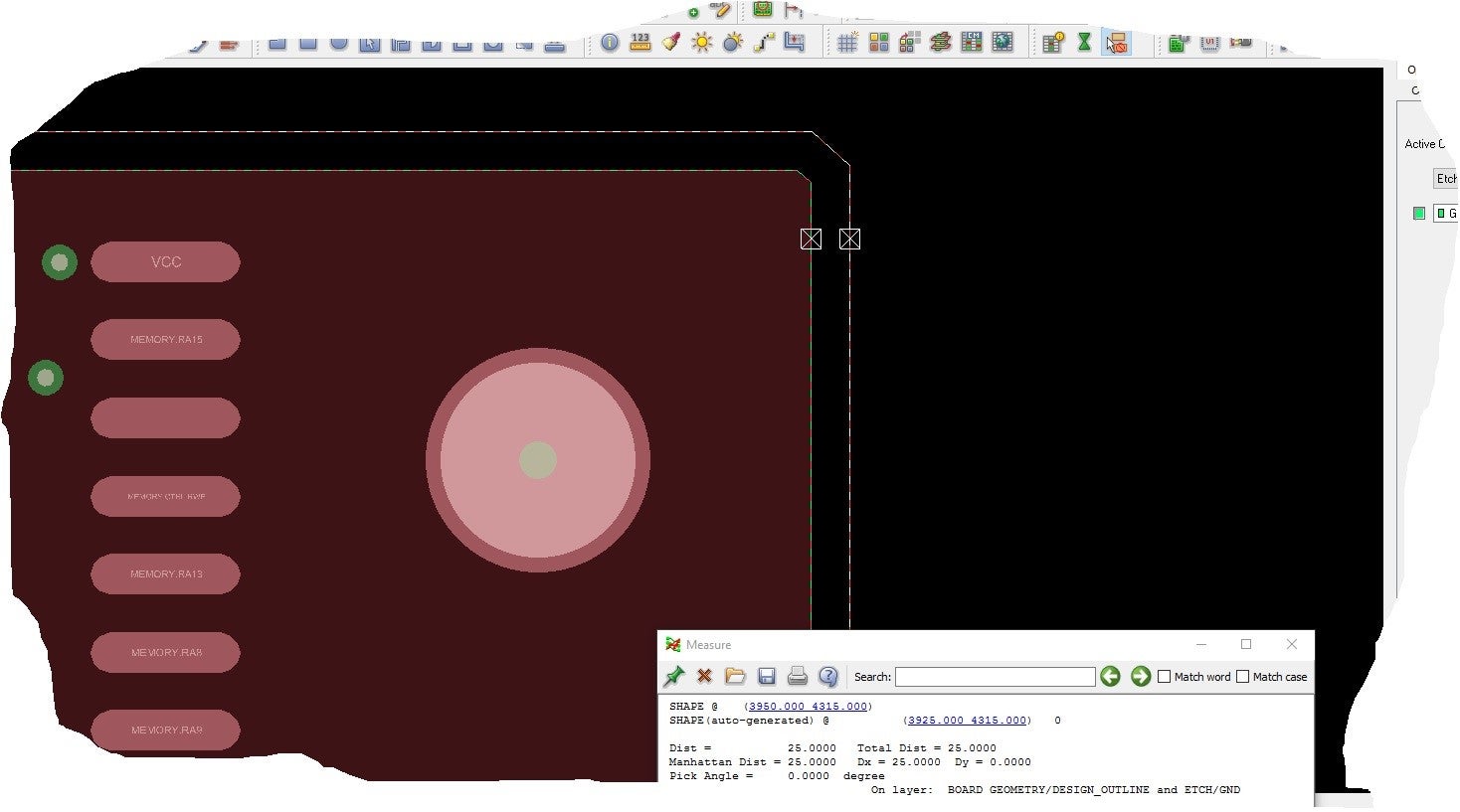
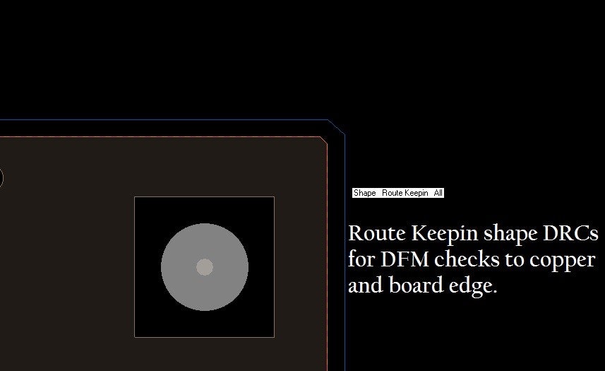
The images above illustrate the relationship between copper areas on your PCBA and the board edge. Part of the PCB creation process includes the motorized transport of boards into acid and wash baths. The copper-to-board edge is the space required to grip the side of the PCB panels to transport the boards throughout the manufacturing process, as well as provide clearance for depanelization—the routing or scoring procedure for separating the panel into individual boards. If the proper spacing between the copper-to-board edge is not set appropriately, manufacturing issues can be created. If the copper is too close to the edge of the board, shorts can be created when the electrical current is applied to the panel during the etching processes.
Note: The equipment used to manufacture the boards will be what controls the spacing needed to grip the panel. Your board fabricator should be able to provide you with design specifications.
Using DRC Checks to Optimize DFM Compliance
The last thing any engineer wants is to receive “the call” from their manufacturer stating their board has failed their DFM checks. So, it is important to look for the above issues in your final checks—whether that’s through automated or manual checks. The consequences of manufacturing failure are not only frustrating, but costly. Planning for the future by designing for manufacturing is just one of the many ways to avoid running into any DFM issues.
The good news is, many of the issues listed above can be automatically identified using an industry-leading EDA design program like OrCAD PCB Designer that comes armed with OrCAD DesignTrueTM In-Design DFM Technology.
It can be a challenge to optimize your design for manufacturability and reap the many benefits; such as faster board spin and bring up and lower costs. With OrCAD’s DesignTrue DFM you can ensure that DFM rules and guidelines are being checked automatically throughout the design process. The alternative to having automated DFM checking capabilities is that you will have to manually identify and resolve them yourself.
EMA Design Automation is a leading provider of the resources that engineers rely on to accelerate innovation. We provide solutions that include PCB design and analysis packages, custom integration software, and engineering expertise, which enable you to create more efficiently. For more information on avoiding DFM issues, please see this e-book and learn how we can help you or your team innovate faster, contact us.