Explosion in the usage of electronic circuit boards over the last couple of decades has significantly raised the functionality of EM products across most industries. It is common for most of us to live or work in an environment that exhibits some degree of ambient intelligence (AmI) or artificial intelligence (AI). For example, ”Alexa, please turn on the lights.” As the demand for smarter and smarter products increases, the capabilities of PCBA design and development tools must improve.
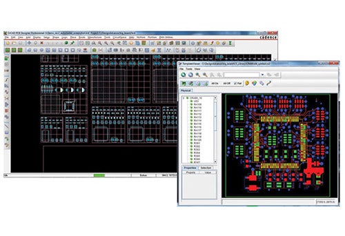
Undoubtedly, EDA packages are significantly more capable and deliver a better UX than their predecessors. This includes free basic programs (often to promote using a particular CAD format or CM engagement). However, the competitiveness of the electronic products industry demands that OEMs, ODMs, and others not only create quality products but strive to optimize quality with time and cost. Many EDA tools are not equipped to achieve this goal. Yet, product design software utilization can overcome common EDA tool limitations.
Limitations of Typical EDA Tools
The basic requirements for a PCBA design program are:
EDA Tool Requirements
1. Schematic capture
- Symbol selection/creation
- Net routing
- Symbol footprint and land pattern matching
2. PCB layout
- Materials selection
- Part placement
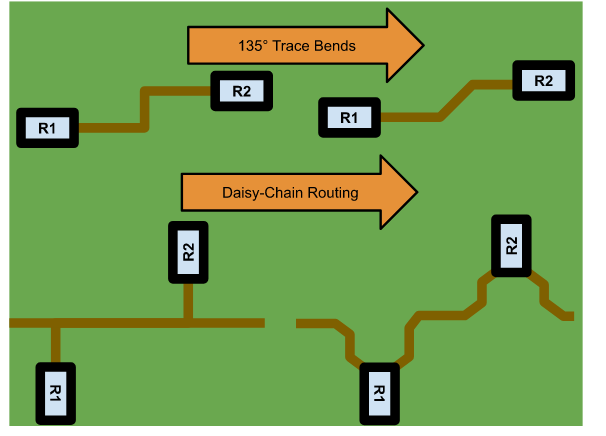
- Trace routing
3. BOM compilation
- MPN listing
- Part location and orientation
- Accurate reference indicators
4. File export
- BOM listing
- Drill hole layout
- PCB layout image
All PCBA programs possess the capabilities listed above. And these are often sufficient to allow for a board to be designed, providing the design is not complex and board specifications don’t extend beyond the equipment capabilities for fabrication and assembly.
Meeting the minimal requirements listed above may get a circuit board built. However, building PCBAs that satisfy performance standards and allow you to compete successfully with other electronics product developers mandates that your development process is optimized to address common EDA tool limitations, as listed below.
Common EDA Tool Limitations
- Lack of supply chain consideration
- No signal and power integrity analysis
- No timing analysis
- No power distribution network and/or thermal analyses
- Restrictive constraint management
- Limited data tracking
- No packaging design capability
- No ECAD/MCAD integration
- Limited or no project library management
Fortunately, these and other shortcomings can be mitigated or eliminated with product development software tools that target virtually every aspect of the PCB design process.
Product Development Software Solutions
EDA program capabilities range from minimal to advanced. The latter includes various functions intended to optimize the design and development process. It reduces the time engineers and designers typically spend on essential tasks like placing components, routing traces, and verifying DFM rules and guideline compliance. These and other capabilities can be acquired for other board design packages by implementing one or more of the product design and development software solutions listed below.
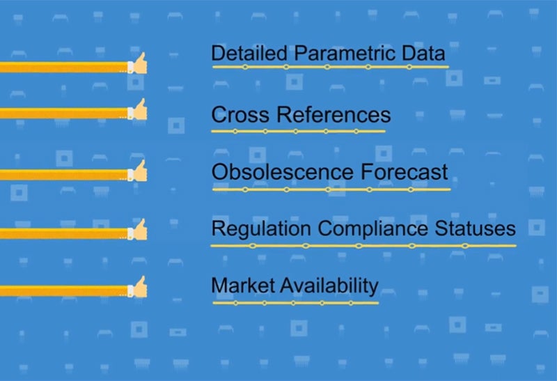
Supply Chain Intelligence
|  |
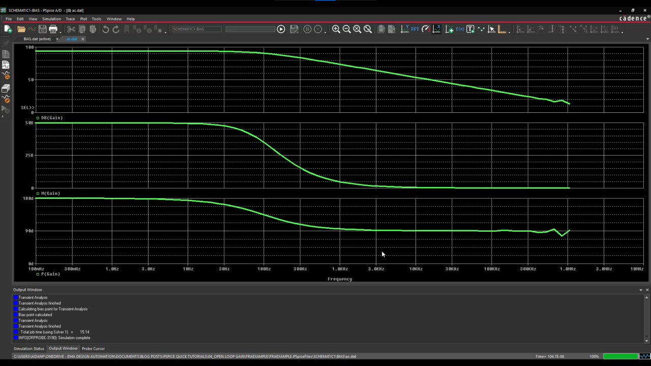 | Mixed Signal Analysis
|
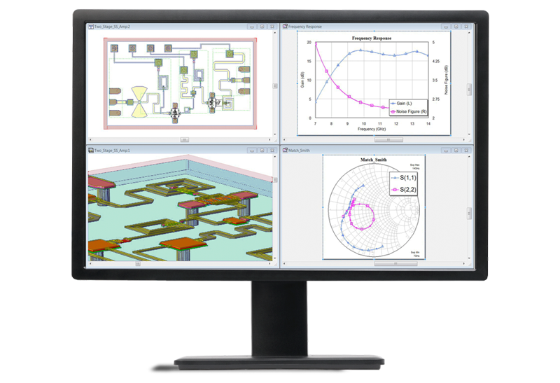
RF and Microwave Simulation
|  |
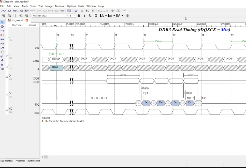 | Timing Analysis
|
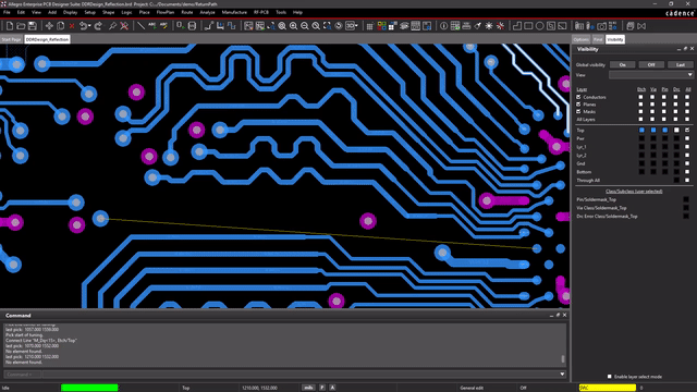
Component Placement and PCB Layout
|  |
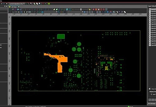
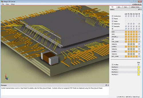
 | Signal and Power Integrity Analysis
|
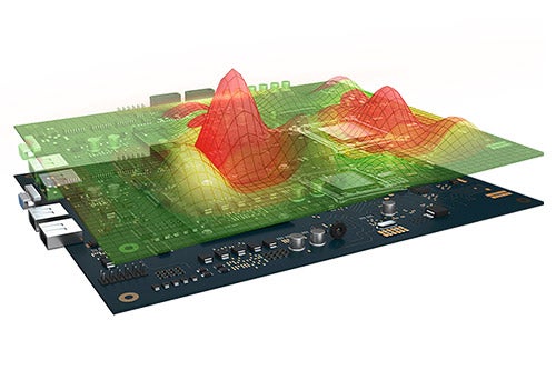
Thermal Simulation and Analyses
|  |
 | Integrated DFM Analysis
|
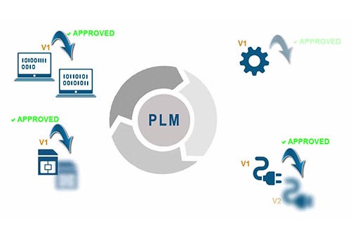
Design Change Tracking
|  |
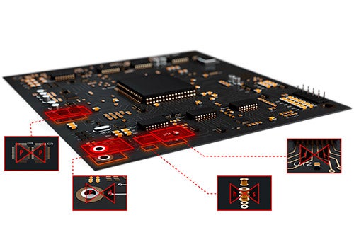
 | Advanced Packaging
|
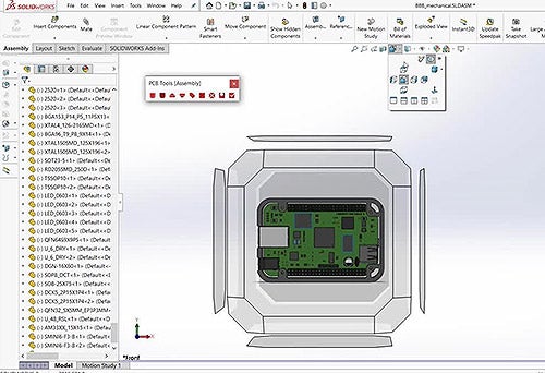
ECAD/MCAD Integration
|  |
 | Project Library Management
|
*Allegro® is an advanced integrated PCB design and analysis platform by Cadence Design Systems, Inc.
As shown above, incorporating solutions like the ones listed above has many advantages that will help you achieve the best balance of quality, time, and cost for your electronic development project.
Selecting the Best EDA Enhancement Tools for Your Project
Product design and development software tools significantly improve the efficiency of your new product introduction (NPI) project. However, select software that integrates well with your EDA package to reap the rewards of these enhancements. Asking the following questions of your provider can help you make a choice that best suits your PCBA or electronic product and optimizes your development process.
Questions for Your Product Design Software Solution Provider
| QUESTIONS | YES |
| Does the program integrate into my design package? If not, do you offer the compatible base EDA package(s)? | ✅ |
| Does the program use industry standard file formats? | ✅ |
| Does the program adhere to pertinent industry standards for my application? | ✅ |
| How steep is the learning curve or how long is the training process? | ✅ |
| Are self-learning aids; such as videos, sample implementations, and a user forum available? | ✅ |
| What type of direct support do you provide? | ✅ |
| Is the program backward/forward compatible? | ✅ |
| Is the program customizable? | ✅ |
Performing research, including asking questions like those above and opting to partner with an experienced EDA enhancement solution provider, will help you ensure that your product design and development software investment delivers the desired process and ROI objectives.
EMA Design Automation is a leading provider of the resources that engineers rely on to accelerate innovation. We provide solutions that include PCB design and analysis packages, custom integration software, and engineering expertise, which enable you to create more efficiently. For more information on product design software and product development software solutions and how we can help you or your team innovate faster, contact us.