What determines a good electronic circuit board design? Or more precisely, what factors should you employ to not only ensure your PCBA will function as intended but will also help facilitate how your board is built? Fortunately, there are rules and specifications intended to meet these objectives. They are commonly referred to as design for manufacturing and assembly guidelines.
Prior to defining DFM and DFA and how to best utilize them, the manufacturing process and the importance of optimizing this stage of the PCBA development process must be explained.
The DBT PCBA Development Cycle
Best practices for designing circuit boards have evolved since their origin in the mid-20th century. Many advances and refinements have occurred as a result of improvements in equipment and/or PCBA design software capabilities. Today, creating electronic circuit boards is typically a complex process that involves three key stages: design, build, and test, as shown in the figure below:
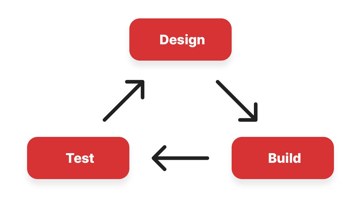
The design⇒build⇒test or DBT cycle is an iterative process where the board design quality is continuously improved until a final prototype or production-ready PCBA is manufactured and validated.
The PCBA development process consists of well-defined steps for manufacturing which must also adhere to industry regulations and standards; such as the performance level classifications defined in IPC-6011 Generic Performance Specification for Printed Boards. This and other publications also serve as the basis for rules that should be employed to guide your design.
Defining DFX
The prevalence of circuit boards is an ever-expanding phenomenon that has an imprint in all aspects of life through the application of electronics to improve the functionality, efficiency, and reliability of products for virtually every industry. This degree of impact means that the PCB industry is a competitive landscape that requires you to design your boards so that the development process and the resulting PCBA are high quality.
The best way to meet this mandate is to employ a philosophy or strategy that includes actions to optimize your board development or to design for excellence (DFX). Focus areas for excellent PCBA design include the following:
Methods to Achieve PCBA Design for Excellence
- Design for manufacturing (DFM)
DFM is the laying out of your circuit board such that the board build process is optimized by choosing specifications that fall within the range of capabilities of your CM’s equipment. - Design for assembly (DFA)
DFA, which is similar to DFM, is making decisions that help facilitate the accurate alignment and mounting of components on your board. - Design for testing (DFT)
DFT is the inclusion of board elements—such as test points or coupons—that enable your board to be tested easily for functionality or structural integrity. - Design for reliability (DFR)
DFR is the incorporation of steps, inspections, and/or analyses to maximize reliability and minimize the possibility that a board will fail to operate as intended—and for the duration of its intended lifecycle once deployed. - Design for cost/procurement (DFC/DFP) DFC/DFP is making design decisions to achieve the best cost-benefit for your board build process. This focus should always be balanced against quality to ensure your PCBAs meet their objectives.
Although, It is a good idea to consider all of the above design focus areas, the level of importance for DFT, DFR, and DFC/DFP may vary depending on your board’s function and application. Manufacturability, however, is always a primary concern and DFM and DFA rules and guidelines should always be followed.
Important DFM Rules You Should Know
There was a time when circuit board design was an isolated exercise where engineers knew very little about how their boards were actually built. Fortunately, this highly inefficient process has been largely replaced with a more transparent designer/manufacturer relationship. With this white box approach, board designers have access to DFM information furnished by fabricators and assemblers that clearly defines acceptable ranges for board specifications that the CM’s equipment can meet.
There are DFM issues that are critical to avoid —such as acid traps, slivers, and solder bridges. However, DFM can cover a much broader range of specifications; including those listed below.
DFM Issues
- Insufficient board edge clearance
- Insufficient spacing between pads
- Insufficient annular ring or via size
- Misaligned via-in-pad
- Incorrect drill hole aspect ratio
For more information on important DFM issues to avoid, see this e-book.
Depending on your service provider—for example, turnkey PCBA manufacturing services—DFM may encompass both PCBA manufacturing stages. In many cases, however, they may be limited to rules and guidelines for fabrication. In these cases, it is necessary for you to acquire DFA rules separately from the assembler. Important guidelines are discussed below.
DFA Guidelines To Prioritize
PCB assembly is the last stage of manufacturing. Therefore, most assembly processes include both manual and optical inspections to ensure that your board includes good solder joints and all components are securely attached. DFA rules that help you avoid the following issues are important to follow.
DFA Issues
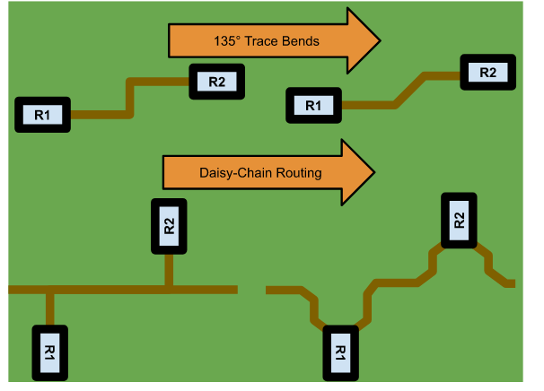
- Misaligned trace and pad
- Incorrect footprint
- Missing solder mask
- Unconnected trace routes
- Improper copper weight
The list above is not exhaustive. In fact, DFA guidelines may include any stipulations that help your CM avoid errors that may help maximize your board’s yield rate—the ratio of boards that are usable to the total number manufactured.
How To Best Implement DFMA Rules and Guidelines
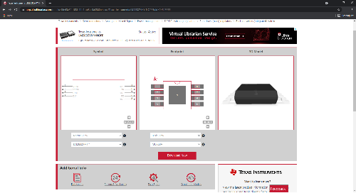
Today, most PCB design software packages include some degree of targeted functionality—such as DRC checks—to assist you in avoiding common design for manufacturing and assembly (DFMA) errors. However, the process for identifying and correcting these errors can be challenging. For example, DRC checks often return a laundry list of flags without any insight as to how to correct them. Additionally, making changes to address one issue will sometimes generate new problems.
OrCAD PCB Designer is the solution to optimizing your DFMA implementation. Not only can you easily upload or create the rules and constraints for your design, but you also get true, real-time, rule-based design. This allows you to make corrections in the process and avoid the endless trial and error that comes with end design-only DRC. And to make sure you get the most from this advanced design suite faster, you should partner with the industry leader in software resources and support for tools like OrCAD.
EMA Design Automation is a leading provider of the resources that engineers rely on to accelerate innovation. We provide solutions that include PCB design and analysis packages, custom integration software, and engineering expertise, which enable you to create more efficiently. For more information on how to best use design for manufacturing and assembly rules, and how we can help you or your team innovate faster, contact us.